ECE 124a/256c VLSI RC(L) Interconnect Models Forrest Brewer

42 Slides913.00 KB
ECE 124a/256c VLSI RC(L) Interconnect Models Forrest Brewer Wayne Burleson, Atul Maheshwari
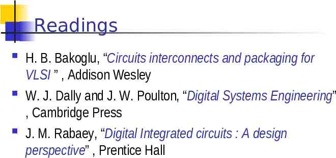
Readings H. B. Bakoglu, “Circuits interconnects and packaging for VLSI ” , Addison Wesley W. J. Dally and J. W. Poulton, “Digital Systems Engineering” , Cambridge Press J. M. Rabaey, “Digital Integrated circuits : A design perspective” , Prentice Hall
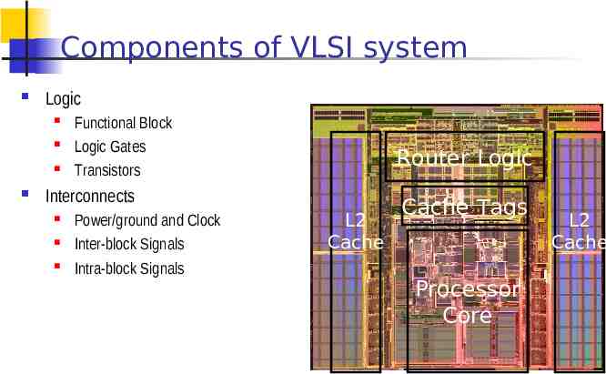
Components of VLSI system Logic Functional Block Logic Gates Transistors Router Logic Interconnects Power/ground and Clock Inter-block Signals Intra-block Signals L2 Cache Cache Tags Processor Core L2 Cache
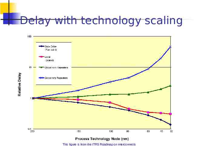
Delay with technology scaling This figure is from the ITRS Roadmap on interconnects
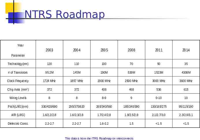
NTRS Roadmap Year 2003 2004 2005 2008 2011 2014 Technology(nm) 120 110 100 70 50 35 # of Transistors 95.2M 145M 190M 539M 1523M 4308M Clock Frequency 1724 MHz 1857 MHz 2000 MHz 2500 MHz 3000 MHz 3600 MHz Chip Area (mm2) 372 372 408 468 536 615 Wiring Levels 8 8 8-9 9 9-10 10 Pitch(L/I/G)(nm) 330/420/690 295/375/620 265/340/560 185/240/390 130/165/275 95/115/190 A/R (L/I/G) 1.6/2.2/2.8 1.6/2.3/2.8 1.7/2.4/2.8 1.9/2.5/2.9 2.1/2.7/3.0 2.3/2.9/3.1 Dielectric Const. 2.2-2.7 2.2-2.7 1.6-2.2 1.5 1.5 1.5 Parameter This data is from the ITRS Roadmap on interconnects
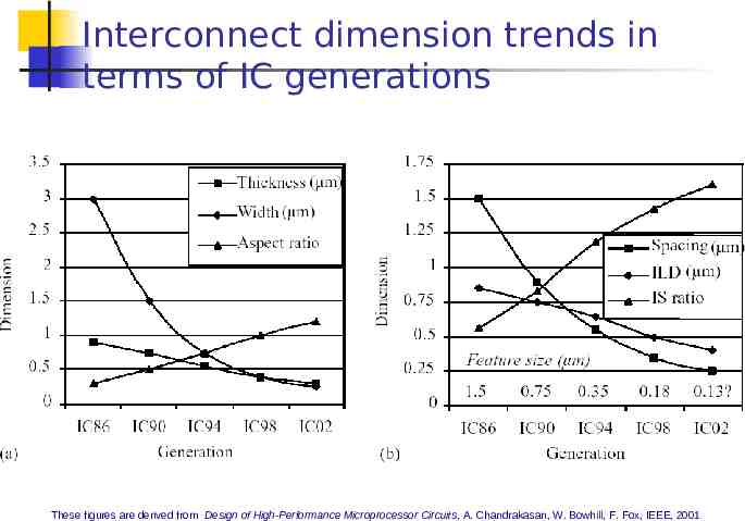
Interconnect dimension trends in terms of IC generations These figures are derived from Design of High-Performance Microprocessor Circuits, A. Chandrakasan, W. Bowhill, F. Fox, IEEE, 2001
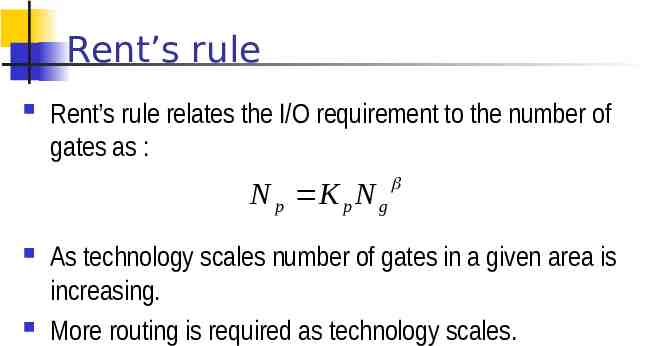
Rent’s rule Rent’s rule relates the I/O requirement to the number of gates as : N p K p N g As technology scales number of gates in a given area is increasing. More routing is required as technology scales.
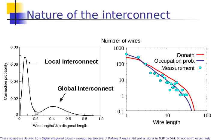
Nature of the interconnect Number of wires 1000 Local Interconnect Donath Occupation prob. Measurement 100 10 Global Interconnect 1 0.1 1 10 Wire length 100 These figures are derived from Digital integrated circuit – a design perspective, J. Rabaey Prentice Hall and a tutorial in SLIP by Dirk Stroobandt respectively
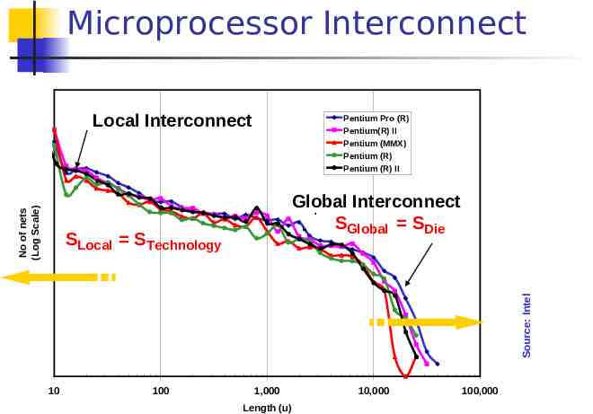
Microprocessor Interconnect No of nets (Log Scale) Local Interconnect Pentium Pro (R) Pentium(R) II Pentium (MMX) Pentium (R) Pentium (R) II Global Interconnect SGlobal SDie Source: Intel SLocal STechnology 10 100 1,000 Length (u) 10,000 100,000
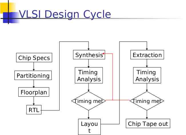
VLSI Design Cycle Chip Specs Synthesis Extraction Partitioning Timing Analysis Timing Analysis Timing met Timing met Layou t Chip Tape out Floorplan RTL
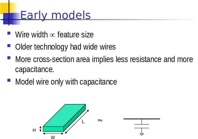
Early models Wire width feature size Older technology had wide wires More cross-section area implies less resistance and more capacitance. Model wire only with capacitance L H W
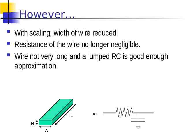
However With scaling, width of wire reduced. Resistance of the wire no longer negligible. Wire not very long and a lumped RC is good enough approximation. L H W
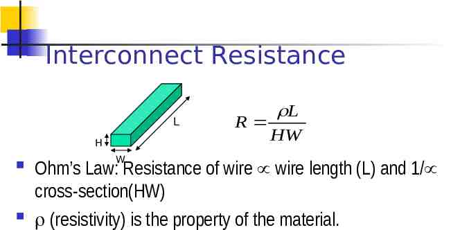
Interconnect Resistance L H W L R HW Ohm’s Law: Resistance of wire wire length (L) and 1/ cross-section(HW) (resistivity) is the property of the material.
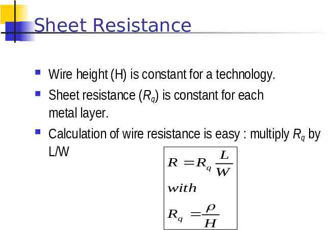
Sheet Resistance Wire height (H) is constant for a technology. Sheet resistance (Rq) is constant for each metal layer. Calculation of wire resistance is easy : multiply Rq by L/W L R Rq W with Rq H
Interconnect Capacitance Capacitance of a wire f (Shape, Distance to surrounding wires, Distance to the substrate ) Estimating Capacitance is a matter of determining where the field lines go. To get an accurate estimate electric field solvers (2D or 3D) are used. E.g. Fastcap or Rafael When in doubt, typical wires have self capacitance between 1 and 3 pf/cm
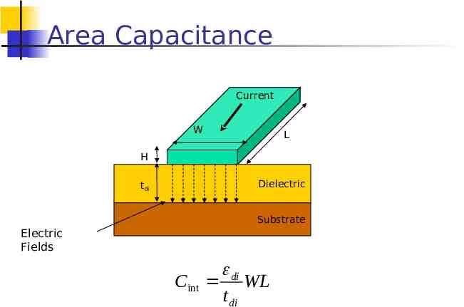
Area Capacitance Current W L H tdi Dielectric Substrate Electric Fields di Cint WL t di
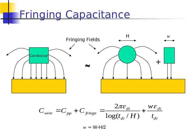
Fringing Capacitance Fringing Fields H w Conductor C wire C pp C fringe 2 di w di log(t di / H ) t di w W-H/2
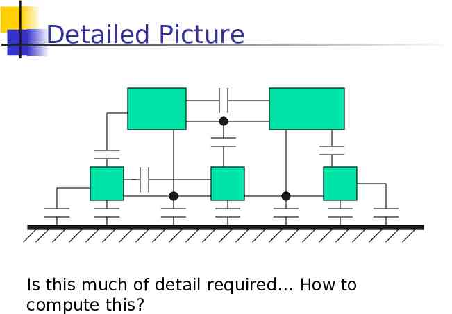
Detailed Picture Is this much of detail required How to compute this?
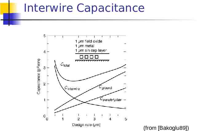
Interwire Capacitance (from [Bakoglu89])
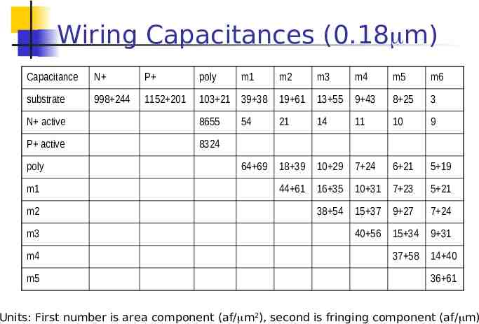
Wiring Capacitances (0.18 m) Capacitance N P poly substrate 998 244 1152 201 m2 m3 m4 m5 m6 103 21 39 38 19 61 13 55 9 43 8 25 3 N active 8655 54 21 14 11 10 9 P active 8324 64 69 18 39 10 29 7 24 6 21 5 19 44 61 16 35 10 31 7 23 5 21 38 54 15 37 9 27 7 24 40 56 15 34 9 31 37 58 14 40 poly m1 m2 m3 m4 m5 m1 36 61 Units: First number is area component (af/ m2), second is fringing component (af/ m)
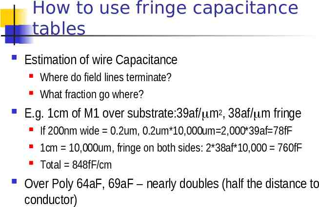
How to use fringe capacitance tables Estimation of wire Capacitance E.g. 1cm of M1 over substrate:39af/ m2, 38af/ m fringe Where do field lines terminate? What fraction go where? If 200nm wide 0.2um, 0.2um*10,000um 2,000*39af 78fF 1cm 10,000um, fringe on both sides: 2*38af*10,000 760fF Total 848fF/cm Over Poly 64aF, 69aF – nearly doubles (half the distance to conductor)
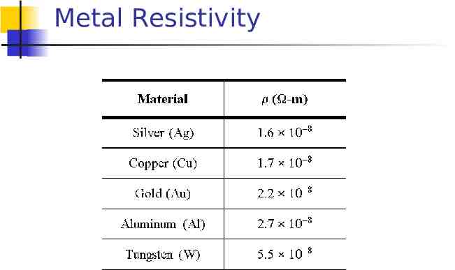
Importance of Resistance Delay of wire to the resistance of the wire. Resistance means ohmic (IR) drop along the wire, reduces noise margin. IR drop a significant problem in the power lines where current density if high. Keep wires short, to reduce resistance. Contact resistance makes them vulnerable to electromigration.
Metal Resistivity
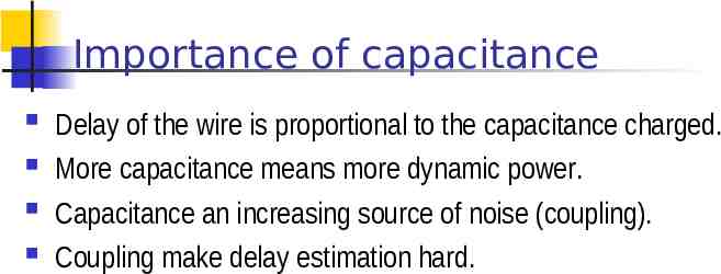
Importance of capacitance Delay of the wire is proportional to the capacitance charged. More capacitance means more dynamic power. Capacitance an increasing source of noise (coupling). Coupling make delay estimation hard.
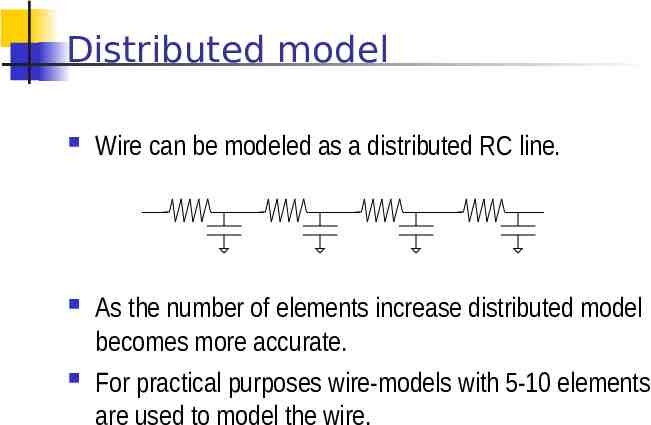
Distributed model Wire can be modeled as a distributed RC line. As the number of elements increase distributed model becomes more accurate. For practical purposes wire-models with 5-10 elements are used to model the wire.
Elmore Delay First order time constant at node is a sum of RC components. All the upstream resistances are taken into account. Thus each node contributes to the delay. Amount of contribution is the product of the cap at the node and the amount of resistance from source to the node.
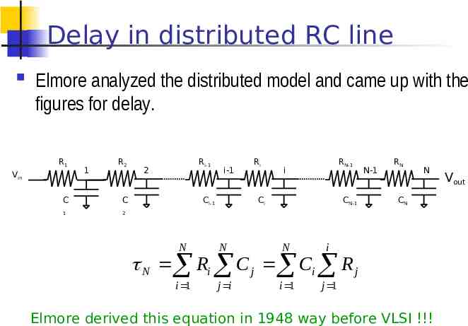
Delay in distributed RC line Elmore analyzed the distributed model and came up with the figures for delay. R1 Vin 1 R2 C C 1 2 Ri-1 2 i-1 Ci-1 Ri RN-1 i Ci CN-1 N N N i i 1 j i i 1 j 1 N-1 RN N CN N Ri C j Ci R j Elmore derived this equation in 1948 way before VLSI !!! Vout
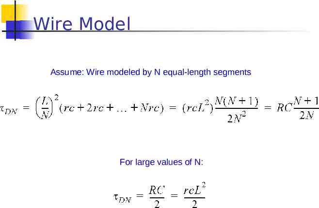
Wire Model Assume: Wire modeled by N equal-length segments For large values of N:
Generalized Elmore delay Rubinstein, Penfield and Horowitz generalized Elmore delay This figure is derived from Digital integrated circuit – a design perspective, J. Rabaey Prentice Hall
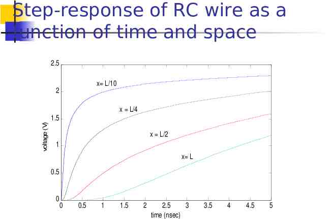
Step-response of RC wire as a function of time and space 2.5 x L/10 2 voltage (V) x L/4 1.5 x L/2 1 x L 0.5 0 0 0.5 1 1.5 2 2.5 3 time (nsec) 3.5 4 4.5 5
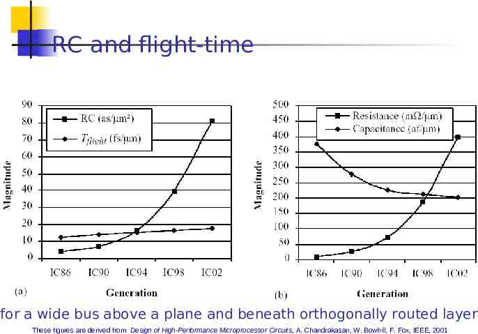
RC and flight-time for a wide bus above a plane and beneath orthogonally routed layer These figures are derived from Design of High-Performance Microprocessor Circuits, A. Chandrakasan, W. Bowhill, F. Fox, IEEE, 2001
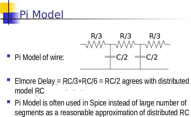
Pi Model R/3 R/3 R/3 Pi Model of wire: Elmore Delay RC/3 RC/6 RC/2 agrees with distributed model RC Pi Model is often used in Spice instead of large number of segments as a reasonable approximation of distributed RC C/2 C/2
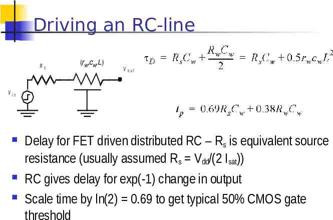
Driving an RC-line Rs (r w,cw,L) V o ut V in Delay for FET driven distributed RC – Rs is equivalent source resistance (usually assumed Rs Vdd/(2 Isat)) RC gives delay for exp(-1) change in output Scale time by ln(2) 0.69 to get typical 50% CMOS gate threshold
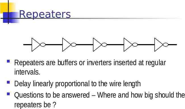
Repeaters Repeaters are buffers or inverters inserted at regular intervals. Delay linearly proportional to the wire length Questions to be answered – Where and how big should the repeaters be ?
Repeater placement Delay of the interconnect is typically optimum when Delaywire Delaybuffer Closed form solutions for Repeater Number and Sizing Bakoglu and Meindl, 1985 (Classical) Adler and Friedman, 1998 (considering inductance) Nalamalpu and Burleson, 2000 (ramped waveforms) Chen Marek-Sadowska, Brewer, 2003 (short channel timing) Cong, 2004 (tapered wires)
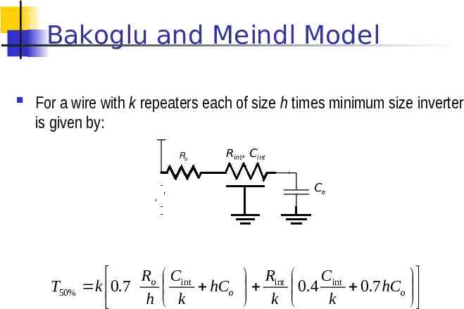
Bakoglu and Meindl Model For a wire with k repeaters each of size h times minimum size inverter is given by: Ro Rint, Cint Co T50% Ro Cint Cint Rint k 0.7 hCo 0.7 hCo 0.4 h k k k
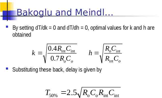
Bakoglu and Meindl By setting dT/dk 0 and dT/dh 0, optimal values for k and h are obtained 0.4 Rint Cint k 0.7 RoCo Ro Cint h Rint Co Substituting these back, delay is given by T50% 2.5 Ro Co Rint Cint
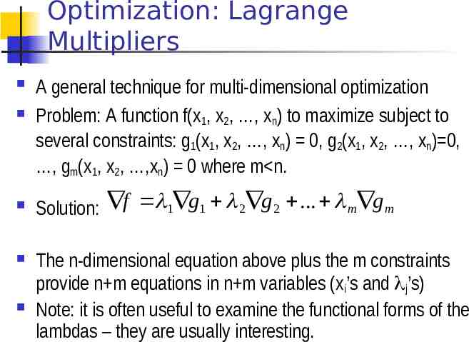
Optimization: Lagrange Multipliers A general technique for multi-dimensional optimization Problem: A function f(x1, x2, , xn) to maximize subject to several constraints: g1(x1, x2, , xn) 0, g2(x1, x2, , xn) 0, , gm(x1, x2, ,xn) 0 where m n. Solution: f 1 g1 2 g 2 . m g m The n-dimensional equation above plus the m constraints provide n m equations in n m variables (xi’s and j’s) Note: it is often useful to examine the functional forms of the lambdas – they are usually interesting.
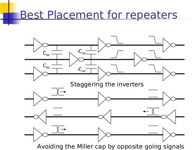
Best Placement for repeaters Clat Clat -Clat -Clat Staggering the inverters Avoiding the Miller cap by opposite going signals
Repeater Design Issues Delay-optimal repeaters are area and power hungry – use of sub-optimal insertion Optimal placement requires accurate modeling of interconnect. Optimal placement not always possible. Performance limited due to significant interconnect resistance. Source of noise – Supply and Substrate
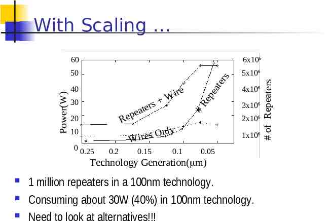
50 5x10⁶ 30 Rep 20 W 0.2 0.15 t er 4x10⁶ 3x10⁶ 2x10⁶ n ly O s e r Wi 10 0 0.25 rs e t ea ire ea 40 0.1 1x10⁶ 0.05 Technology Generation( m) 1 million repeaters in a 100nm technology. Consuming about 30W (40%) in 100nm technology. Need to look at alternatives!!! # of Repeaters 6x10⁶ s 60 #R ep Power(W) With Scaling
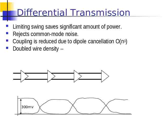
Differential Transmission Limiting swing saves significant amount of power. Rejects common-mode noise. Coupling is reduced due to dipole cancellation O(n3) Doubled wire density -- 300mv