DSP Tutorial Version Date Author Notes 1.0 Jan, 2014 Yiwei Ma First
43 Slides2.06 MB
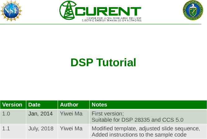
DSP Tutorial Version Date Author Notes 1.0 Jan, 2014 Yiwei Ma First version; Suitable for DSP 28335 and CCS 5.0 1.1 July, 2018 Yiwei Ma Modified template, adjusted slide sequence, Added instructions to the sample code
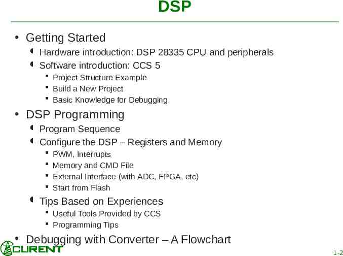
DSP Getting Started Hardware introduction: DSP 28335 CPU and peripherals Software introduction: CCS 5 Project Structure Example Build a New Project Basic Knowledge for Debugging DSP Programming Program Sequence Configure the DSP – Registers and Memory PWM, Interrupts Memory and CMD File External Interface (with ADC, FPGA, etc) Start from Flash Tips Based on Experiences Useful Tools Provided by CCS Programming Tips Debugging with Converter – A Flowchart 1-2
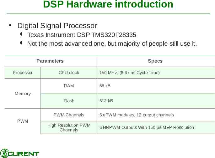
DSP Hardware introduction Digital Signal Processor Texas Instrument DSP TMS320F28335 Not the most advanced one, but majority of people still use it. Parameters Processor Specs CPU clock 150 MHz, (6.67 ns Cycle Time) RAM 68 kB Flash 512 kB Memory PWM Channels PWM High Resolution PWM Channels 6 ePWM modules, 12 output channels 6 HRPWM Outputs With 150 ps MEP Resolution
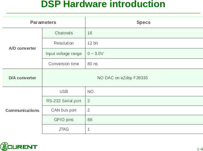
DSP Hardware introduction Parameters Specs Channels 16 Resolution 12 bit A/D converter Input voltage range Conversion time 0 3.0V 80 ns D/A converter NO DAC on eZdsp F28335 USB Communications NO RS-232 Serial port 2 CAN bus port 2 GPIO pins 88 JTAG 1 1-4
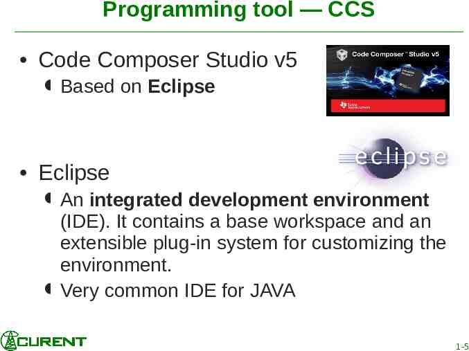
Programming tool — CCS Code Composer Studio v5 Based on Eclipse Eclipse An integrated development environment (IDE). It contains a base workspace and an extensible plug-in system for customizing the environment. Very common IDE for JAVA 1-5
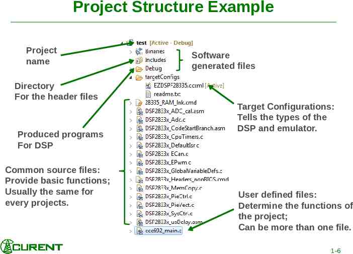
Project Structure Example Project name Directory For the header files Produced programs For DSP Common source files: Provide basic functions; Usually the same for every projects. Software generated files Target Configurations: Tells the types of the DSP and emulator. User defined files: Determine the functions of the project; Can be more than one file. 1-6
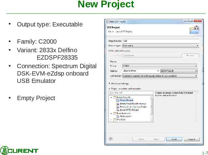
New Project Output type: Executable Family: C2000 Variant: 2833x Delfino EZDSPF28335 Connection: Spectrum Digital DSK-EVM-eZdsp onboard USB Emulator Empty Project 1-7
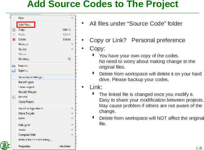
Add Source Codes to The Project All files under “Source Code” folder Copy or Link? Personal preference Copy: You have your own copy of the codes. No need to worry about making change to the original files. Delete from workspace will delete it on your hard drive. Please backup your codes. Link: The linked file is changed once you modify it. Easy to share your modification between projects. May cause problem if others are not aware of the change. Delete from workspace will NOT affect the original file. 1-8
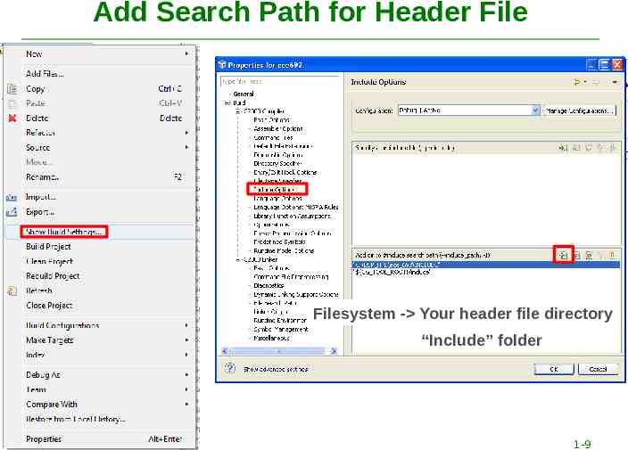
Add Search Path for Header File Filesystem - Your header file directory “Include” folder 1-9
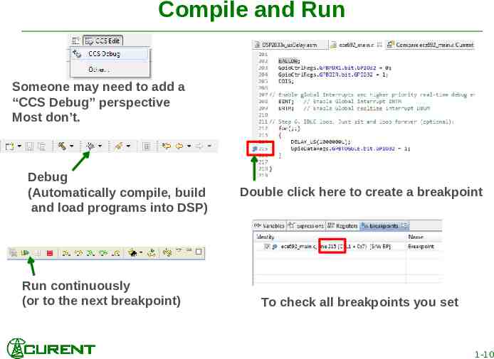
Compile and Run Someone may need to add a “CCS Debug” perspective Most don’t. Debug (Automatically compile, build and load programs into DSP) Run continuously (or to the next breakpoint) Double click here to create a breakpoint To check all breakpoints you set 1-10
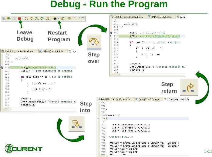
Debug - Run the Program Leave Debug Restart Program Step over Step return Step into 1-11
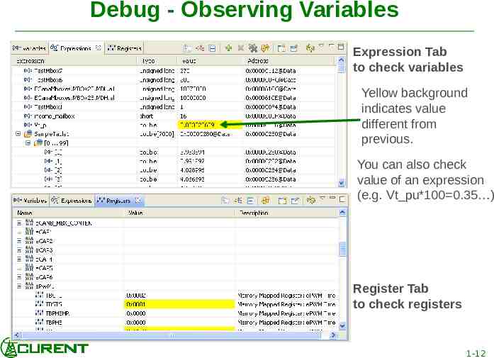
Debug - Observing Variables Expression Tab to check variables Yellow background indicates value different from previous. You can also check value of an expression (e.g. Vt pu*100 0.35 ) Register Tab to check registers 1-12
DSP Programming Program Sequence Configure the DSP – Registers and Memory PWM, Interrupts Memory and CMD File External Interface (with ADC, FPGA, etc) Start from Flash Tips Based on Experiences Useful Tools Provided by CCS Programming Tips 1-13
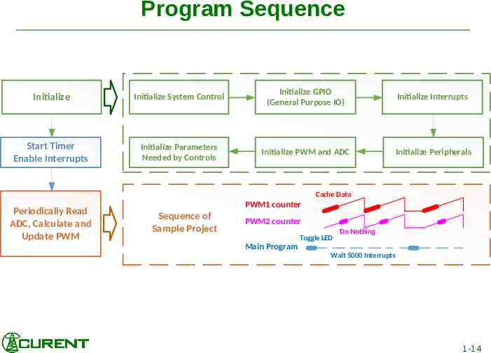
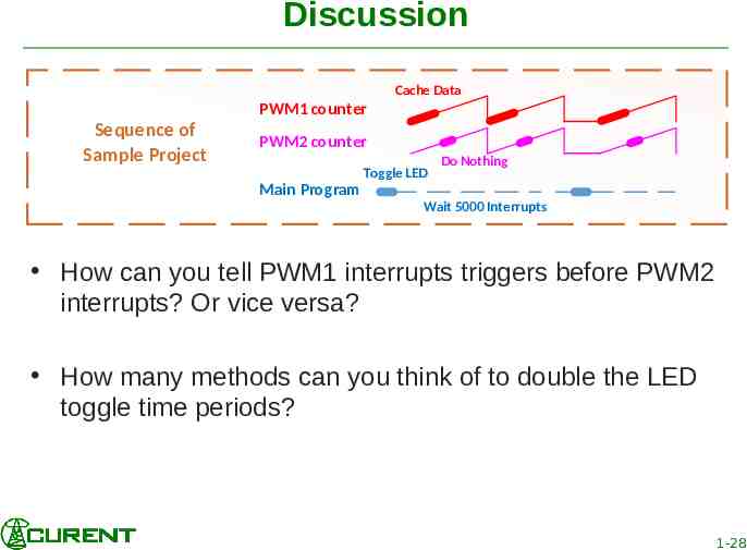
Program Sequence Initialize Initialize System Control Initialize GPIO (General Purpose IO) Initialize Interrupts Start Timer Enable Interrupts Initialize Parameters Needed by Controls Initialize PWM and ADC Initialize Peripherals Cache Data Periodically Read ADC, Calculate and Update PWM PWM1 counter Sequence of Sample Project PWM2 counter Toggle LED Do Nothing Main Program Wait 5000 Interrupts 1-14
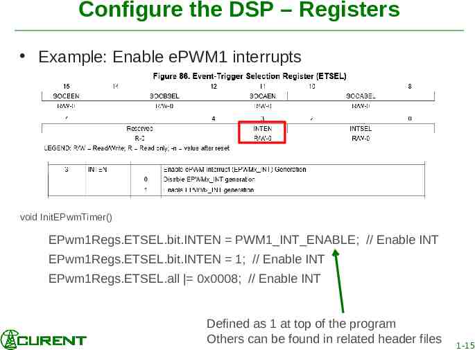
Configure the DSP – Registers Example: Enable ePWM1 interrupts void InitEPwmTimer() EPwm1Regs.ETSEL.bit.INTEN PWM1 INT ENABLE; // Enable INT EPwm1Regs.ETSEL.bit.INTEN 1; // Enable INT EPwm1Regs.ETSEL.all 0x0008; // Enable INT Defined as 1 at top of the program Others can be found in related header files 1-15
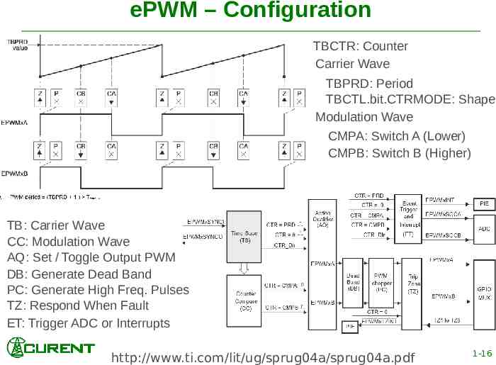
ePWM – Configuration TBCTR: Counter Carrier Wave TBPRD: Period TBCTL.bit.CTRMODE: Shape Modulation Wave CMPA: Switch A (Lower) CMPB: Switch B (Higher) TB: Carrier Wave CC: Modulation Wave AQ: Set / Toggle Output PWM DB: Generate Dead Band PC: Generate High Freq. Pulses TZ: Respond When Fault ET: Trigger ADC or Interrupts http://www.ti.com/lit/ug/sprug04a/sprug04a.pdf 1-16
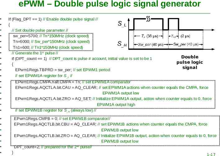
ePWM – Double pulse logic signal generator If (Flag DPT 1) // Enable double pulse signal // { // Set double pulse parameter // sw per 5700; // Tn*150MHz (clock speed) Tn 6000; // Sw per*150MHz (clock speed) Tn1 600; // Tn1*150MHz (clock speed) // Generate the 1st pulse // if (DPT count 1) // DPT count is pulse # account, initial value is set to be 1 { EPwm1Regs.TBPRD sw per; // set EPWM1 period // set EPWM1A register for S L // Double pulse logic signal EPwm1Regs.CMPA.half.CMPA Tn; // set EPWM1A comparator EPwm1Regs.AQCTLA.bit.CAU AQ CLEAR; // set EPWM1A actions when counter equals the CMPA, force EPWM1A output low EPwm1Regs.AQCTLA.bit.ZRO AQ SET; // Initialize EPWM1A output, action when counter equals to 0, force EPWM1A output high // set EPWM1B register for S H (always low) // EPwm1Regs.CMPB 0; // set EPWM1B comparator// EPwm1Regs.AQCTLB.bit.CBU AQ CLEAR; // set EPWM1B actions when counter equals the CMPA, force EPWM1B output low EPwm1Regs.AQCTLB.bit.ZRO AQ CLEAR; // Initialize EPWM1B output, action when counter equals to 0, force EPWM1B output low DPT count 2; // prepared for the 2nd pulse// } 1-17
ePWM – Double pulse logic signal generator else // Generate the 2nd pulse // { if (DPT count 2) { EPwm1Regs.TBPRD sw per; // set EPWM1 period EPwm1Regs.CMPA.half.CMPA Tn1; // re-set EPWM1A comparator EPwm1Regs.CMPB 0; // set EPWM1B comparator DPT count 3; // Complete double pulse signal generator// } else // After the 2nd pulse, disable PWM output { EPwm1Regs.TBPRD sw per; // set EPWM1 period EPwm1Regs.CMPA.half.CMPA 0; // re-set EPWM1A comparator EPwm1Regs.AQCTLA.bit.ZRO AQ CLEAR; // Initialize EPWM1A output, action when counter equals to 0 force EPWM1A output low EPwm1Regs.CMPB 0; // set EPWM1B comparator } } 1-18
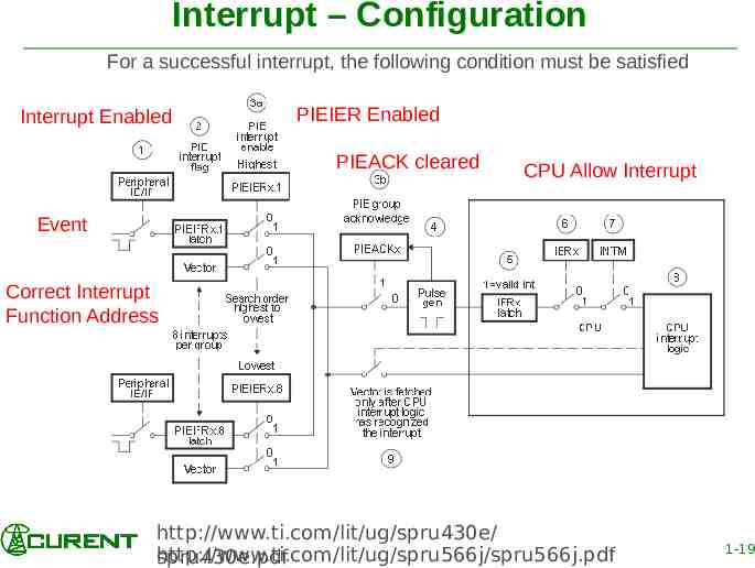
Interrupt – Configuration For a successful interrupt, the following condition must be satisfied Interrupt Enabled PIEIER Enabled PIEACK cleared CPU Allow Interrupt Event Correct Interrupt Function Address http://www.ti.com/lit/ug/spru430e/ http://www.ti.com/lit/ug/spru566j/spru566j.pdf spru430e.pdf 1-19
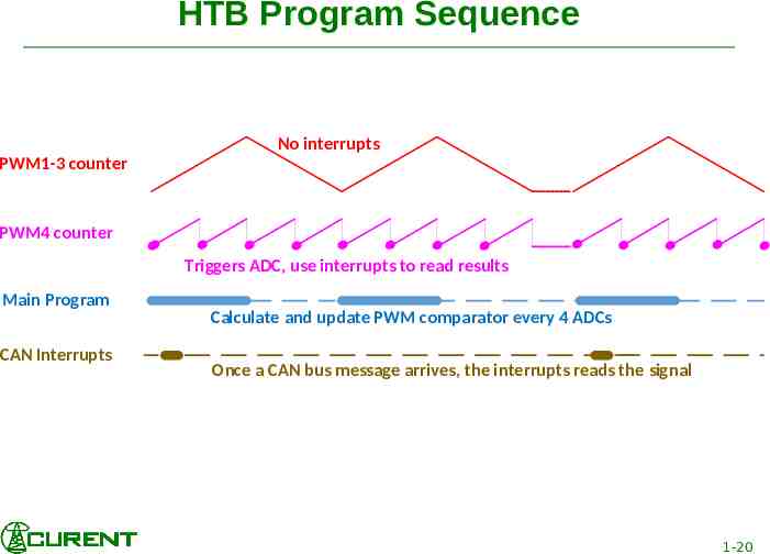
HTB Program Sequence No interrupts PWM1-3 counter PWM4 counter Triggers ADC, use interrupts to read results Main Program CAN Interrupts Calculate and update PWM comparator every 4 ADCs Once a CAN bus message arrives, the interrupts reads the signal 1-20
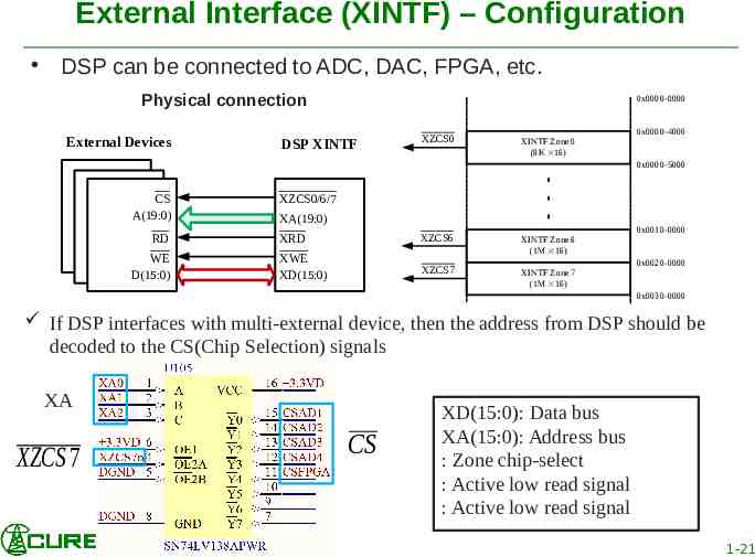
External Interface (XINTF) – Configuration DSP can be connected to ADC, DAC, FPGA, etc. Physical connection External Devices 0x0000-0000 DSP XINTF XZCS0 XINTF Zone 0 (8K 16) 0x0000-4000 0x0000-5000 CS A(19:0) RD WE D(15:0) XZCS0/6/7 XA(19:0) XRD XZCS6 XWE XD(15:0) XINTF Zone 6 (1M 16) XZCS7 XINTF Zone 7 (1M 16) 0x0010-0000 0x0020-0000 0x0030-0000 If DSP interfaces with multi-external device, then the address from DSP should be decoded to the CS(Chip Selection) signals XA XZCS 7 CS XD(15:0): Data bus XA(15:0): Address bus : Zone chip-select : Active low read signal : Active low read signal 1-21
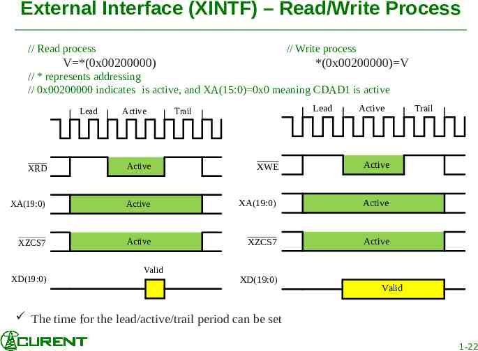
External Interface (XINTF) – Read/Write Process // Read process // Write process V *(0x00200000) *(0x00200000) V // * represents addressing // 0x00200000 indicates is active, and XA(15:0) 0x0 meaning CDAD1 is active Lead Active Lead Trail Active XRD Active XWE Active XA(19:0) Active XA(19:0) Active XZCS7 Active XZCS7 Active XD(19:0) Valid XD(19:0) Trail Valid The time for the lead/active/trail period can be set 1-22
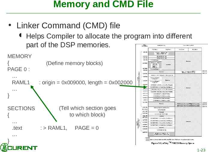
Memory and CMD File Linker Command (CMD) file Helps Compiler to allocate the program into different part of the DSP memories. MEMORY { PAGE 0 : RAML1 } (Define memory blocks) : origin 0x009000, length 0x002000 (Tell which section goes SECTIONS to which block) { .text : RAML1, PAGE 0 } 1-23
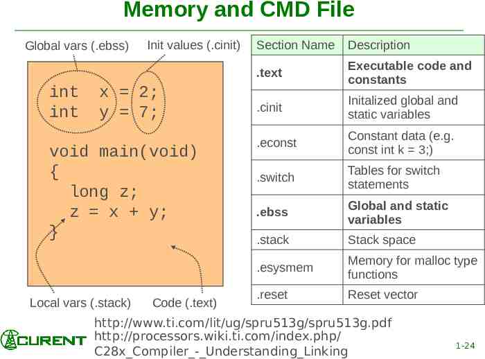
Memory and CMD File Global vars (.ebss) int int Init values (.cinit) x 2; y 7; void main(void) { long z; z x y; } Local vars (.stack) Code (.text) Section Name Description .text Executable code and constants .cinit Initalized global and static variables .econst Constant data (e.g. const int k 3;) .switch Tables for switch statements .ebss Global and static variables .stack Stack space .esysmem Memory for malloc type functions .reset Reset vector http://www.ti.com/lit/ug/spru513g/spru513g.pdf http://processors.wiki.ti.com/index.php/ C28x Compiler - Understanding Linking 1-24
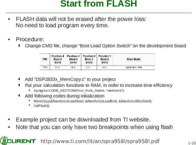
Start from FLASH FLASH data will not be erased after the power loss: No need to load program every time. Procedure: Change CMD file, change “Boot Load Option Switch” on the development board Add “DSP2833x MemCopy.c” to your project Put your calculation functions to RAM, in order to increase time efficiency #pragma CODE SECTION(Your Func Name, "ramfuncs"); Add following codes during initialization MemCopy(&RamfuncsLoadStart, &RamfuncsLoadEnd, &RamfuncsRunStart); InitFlash(); Example project can be downloaded from TI website. Note that you can only have two breakpoints when using flash http://www.ti.com/lit/an/spra958l/spra958l.pdf 1-25
What Could Go Wrong If there are errors or warnings shown. Google it, or ask in forums If there are no explicit errors, but running have problems, generally possible reasons are: Broken DSP / Bad configuration on CCS / Emulator Breakpoints do not work (Programs run well) Jumper on Development Board is not set correctly Related registers are configured wrong or didn’t manually clear after an event. 1-26
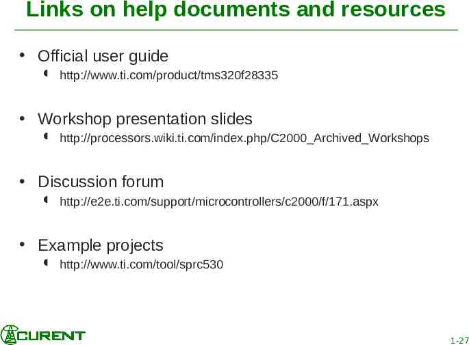
Links on help documents and resources Official user guide http://www.ti.com/product/tms320f28335 Workshop presentation slides http://processors.wiki.ti.com/index.php/C2000 Archived Workshops Discussion forum http://e2e.ti.com/support/microcontrollers/c2000/f/171.aspx Example projects http://www.ti.com/tool/sprc530 1-27
Discussion Cache Data PWM1 counter Sequence of Sample Project PWM2 counter Toggle LED Do Nothing Main Program Wait 5000 Interrupts How can you tell PWM1 interrupts triggers before PWM2 interrupts? Or vice versa? How many methods can you think of to double the LED toggle time periods? 1-28
Useful Functions Plot Graph from Cached Data Save Cached Data Compare with Local History Memory Browser Search All Files in Workspace Useful Shortcut Keys Clock 1-29
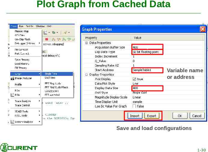
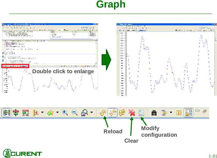
Plot Graph from Cached Data 0 Variable name or address Save and load configurations 1-30
Graph Double click to enlarge Reload Clear Modify configuration 1-31
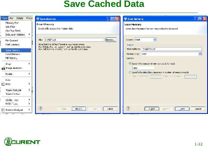
Save Cached Data 1-32
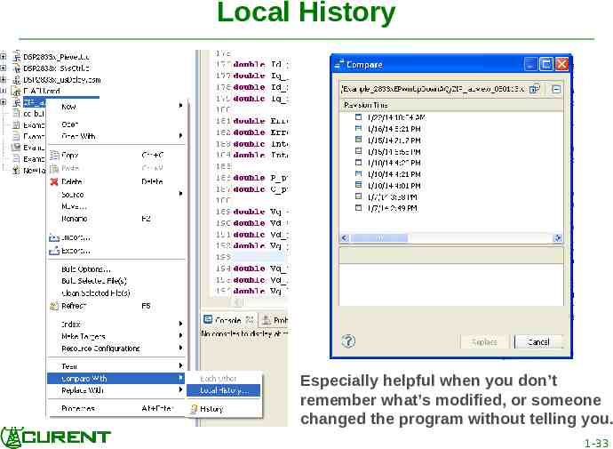
Local History Especially helpful when you don’t remember what’s modified, or someone changed the program without telling you. 1-33
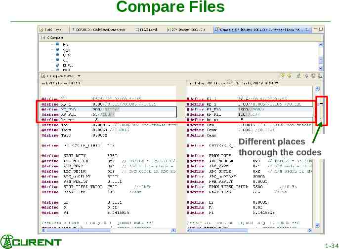
Compare Files Different places thorough the codes 1-34
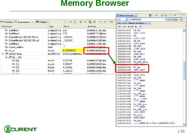
Memory Browser 1-35
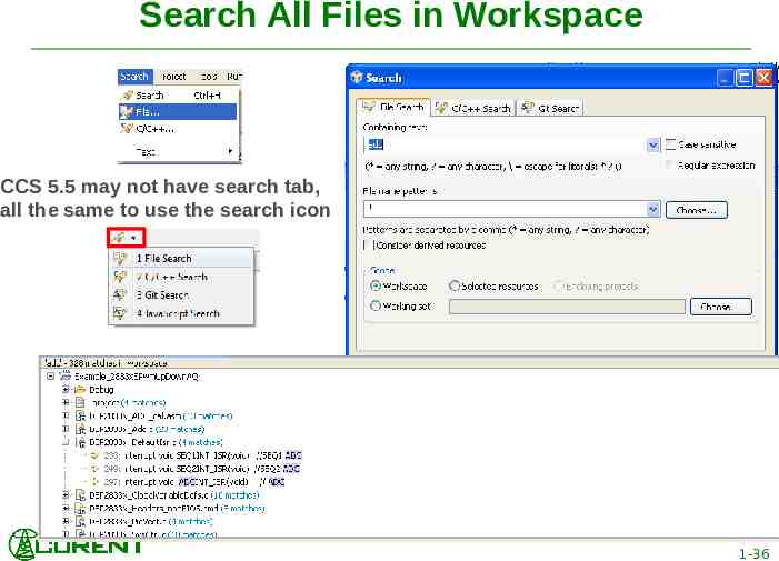
Search All Files in Workspace CCS 5.5 may not have search tab, all the same to use the search icon 1-36
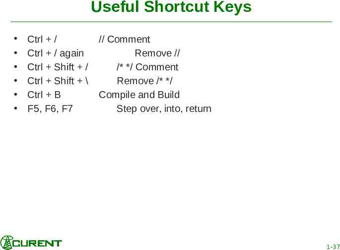
Useful Shortcut Keys Ctrl / Ctrl / again Ctrl Shift / Ctrl Shift \ Ctrl B F5, F6, F7 // Comment Remove // /* */ Comment Remove /* */ Compile and Build Step over, into, return 1-37
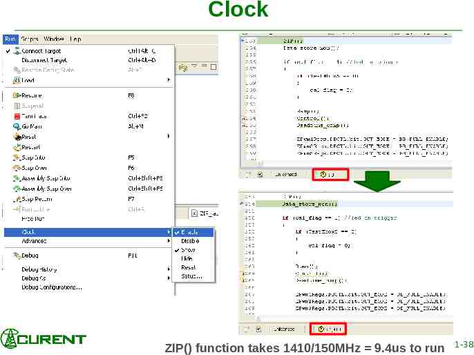
Clock ZIP() function takes 1410/150MHz 9.4us to run 1-38
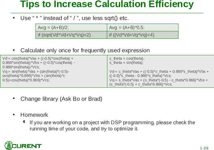
Tips to Increase Calculation Efficiency Use “ * ” instead of “ / ”, use less sqrt() etc. Avg (A B)/2; Avg (A B)*0.5; if (sqrt(Vd*Vd Vq*Vq) 2) if ((Vd*Vd Vq*Vq) 4) Calculate only once for frequently used expression Vd cos(theta)*Vas ((-0.5)*cos(theta) 0.866*sin(theta))*Vbs ((-0.5)*cos(theta) 0.866*sin(theta))*Vcs; Vq sin(theta)*Vas (sin(theta)*(-0.5)cos(theta)*0.866)*Vbs (sin(theta)*(0.5) cos(theta)*0.866)*Vcs; Change library (Ask Bo or Brad) Homework c theta cos(theta); s theta sin(theta); Vd c theta*Vas ((-0.5)*c theta 0.866*s theta)*Vbs ((-0.5)*c theta - 0.866*s theta)*Vcs; Vq s theta*Vas (s theta*(-0.5) - c theta*0.866)*Vbs (s theta*(-0.5) c theta*0.866)*Vcs; If you are working on a project with DSP programming, please check the running time of your code, and try to optimize it. 1-39
Tips on Programming Readability Comments Good example from Zheyu’s double pulse program Meaningful variable and function names Indentation 1-40
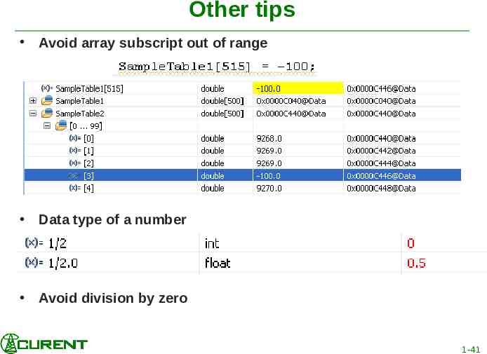
Other tips Avoid array subscript out of range Data type of a number Avoid division by zero 1-41
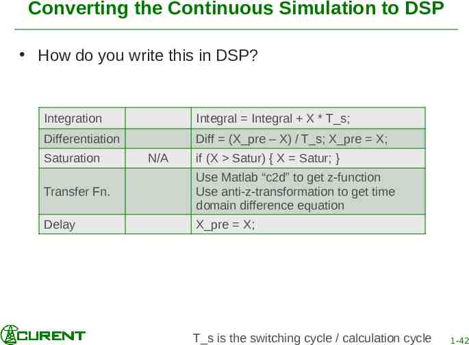
Converting the Continuous Simulation to DSP How do you write this in DSP? Integration Integral Integral X * T s; Differentiation Diff (X pre – X) / T s; X pre X; Saturation N/A if (X Satur) { X Satur; } Transfer Fn. Use Matlab “c2d” to get z-function Use anti-z-transformation to get time domain difference equation Delay X pre X; T s is the switching cycle / calculation cycle 1-42
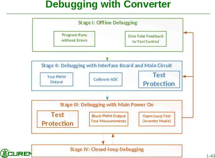
Debugging with Converter Stage I: Offline Debugging Program Runs without Errors Give Fake Feedback to Test Control Stage II: Debugging with Interface Board and Main Circuit Test PWM Output Calibrate ADC Test Protection Stage III: Debugging with Main Power On Test Protection Block PWM Output Test Measurements Open Loop Test (Inverter Mode) Stage IV: Closed-loop Debugging 1-43