Lecture 1 Introduction to Digital Logic Design Hai Zhou EECS 303


30 Slides351.50 KB
Lecture 1 Introduction to Digital Logic Design Hai Zhou EECS 303 Advanced Digital Design Fall 2011 EECS 303 Lecture 1 1
Outline Class administration Digital design methodology Representations of Digital Design Introduction to Mentor Graphics tools READING: – Chapter 1 – Chapter 2 EECS 303 Lecture 1 2
Class Administration Lectures twice a week, Tuesday-Thursday 3:30-4:50PM Instructor: – – – – Hai Zhou Office: L461 Tech EMAIL: [email protected] PHONE: 491-4155 Teaching Assistant – Peng Kang – Office: M314 Tech – EMAIL: [email protected] Web Page: www.eecs.northestern.edu/ haizhou/303/ EECS 303 Lecture 1 3
Class Prerequisites EECS 203: Introduction to Computer Engineering – Need to have basic understanding of digital systems, logic gates, combinational and sequential logic Need to have been exposed to UNIX since we will use the Mentor Graphics tools on SUN workstations Class will form a background for other classes in Computer Engineering – – – – EECS 357: Introduction to VLSI CAD EECS 355: ASIC & FPGA Design EECS 361: Computer Architecture EECS 391: Introduction to VLSI Design EECS 303 Lecture 1 4
Class Administration Required Textbooks: – Mano and Kime, “Logic & Computer Design Fundamentals”, Prentice Hall. Classnotes – Copies of lecture transparencies to be made available EECS 303 Lecture 1 5
Class Grades 5 Homeworks – 25% of grade 5 Labs – 25% of grade Midterm exam – 20% of grade Final exam – 30% of grade Homeworks and labs will be due at the beginning of class on the due date – A penalty of 10% per working day will be assigned to late assignments or labs EECS 303 Lecture 1 6
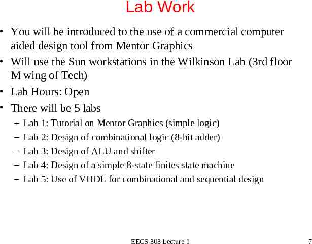
Lab Work You will be introduced to the use of a commercial computer aided design tool from Mentor Graphics Will use the Sun workstations in the Wilkinson Lab (3rd floor M wing of Tech) Lab Hours: Open There will be 5 labs – – – – – Lab 1: Tutorial on Mentor Graphics (simple logic) Lab 2: Design of combinational logic (8-bit adder) Lab 3: Design of ALU and shifter Lab 4: Design of a simple 8-state finites state machine Lab 5: Use of VHDL for combinational and sequential design EECS 303 Lecture 1 7
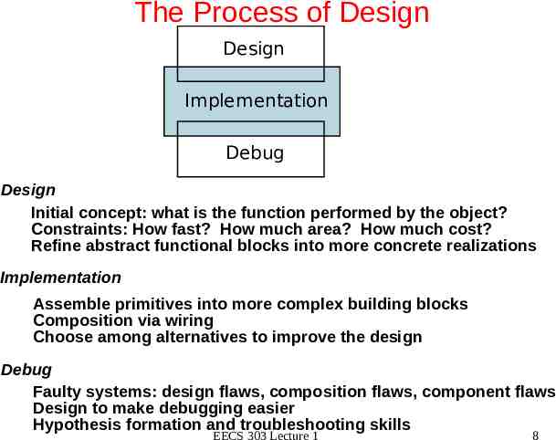
The Process of Design Design Implementation Debug Design Initial concept: what is the function performed by the object? Constraints: How fast? How much area? How much cost? Refine abstract functional blocks into more concrete realizations Implementation Assemble primitives into more complex building blocks Composition via wiring Choose among alternatives to improve the design Debug Faulty systems: design flaws, composition flaws, component flaws Design to make debugging easier Hypothesis formation and troubleshooting skills EECS 303 Lecture 1 8
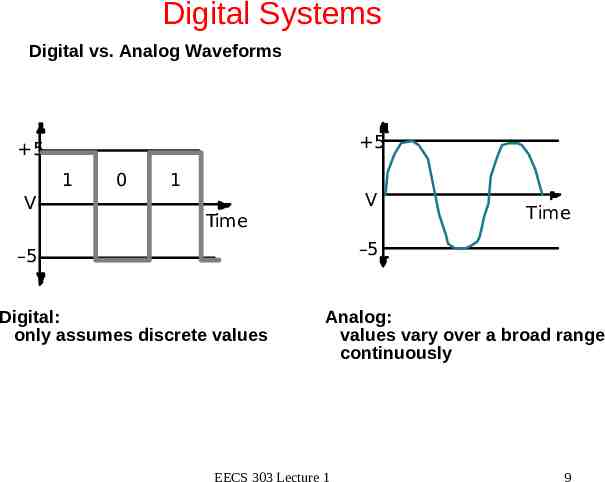
Digital Systems Digital vs. Analog Waveforms 5 5 1 V 0 1 V Time Time –5 –5 Digital: only assumes discrete values Analog: values vary over a broad range continuously EECS 303 Lecture 1 9
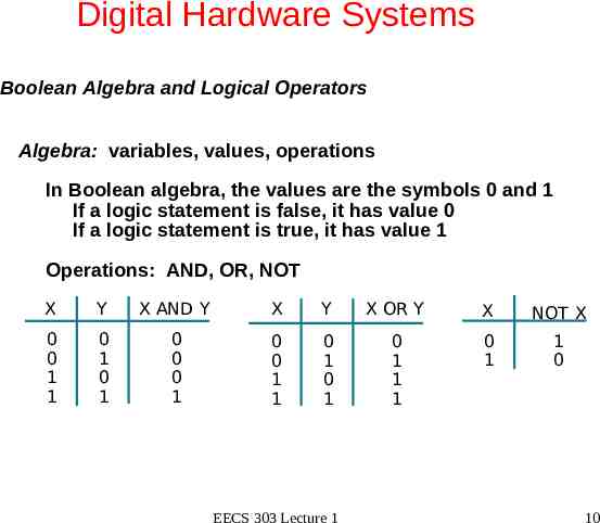
Digital Hardware Systems Boolean Algebra and Logical Operators Algebra: variables, values, operations In Boolean algebra, the values are the symbols 0 and 1 If a logic statement is false, it has value 0 If a logic statement is true, it has value 1 Operations: AND, OR, NOT X Y X AND Y X Y X OR Y X NOT X 0 0 1 1 0 1 0 1 0 0 0 1 0 0 1 1 0 1 0 1 0 1 1 1 0 1 1 0 EECS 303 Lecture 1 10
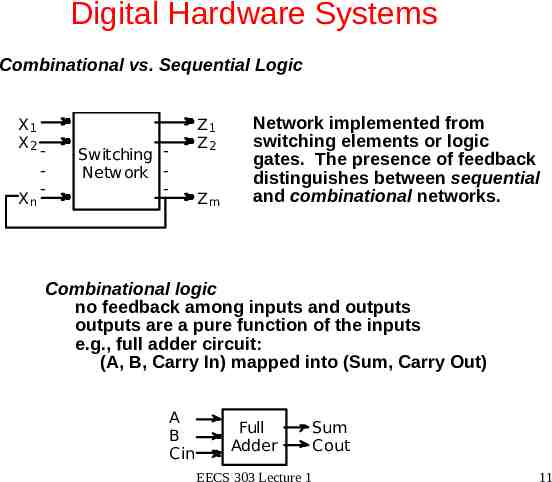
Digital Hardware Systems Combinational vs. Sequential Logic X1 X2 Xn - Switching Network - Z1 Z2 Zm Network implemented from switching elements or logic gates. The presence of feedback distinguishes between sequential and combinational networks. Combinational logic no feedback among inputs and outputs outputs are a pure function of the inputs e.g., full adder circuit: (A, B, Carry In) mapped into (Sum, Carry Out) A B Cin Full Adder EECS 303 Lecture 1 Sum Cout 11
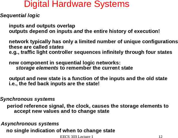
Digital Hardware Systems Sequential logic inputs and outputs overlap outputs depend on inputs and the entire history of execution! network typically has only a limited number of unique configurations these are called states e.g., traffic light controller sequences infinitely through four states new component in sequential logic networks: storage elements to remember the current state output and new state is a function of the inputs and the old state i.e., the fed back inputs are the state! Synchronous systems period reference signal, the clock, causes the storage elements to accept new values and to change state Asynchronous systems no single indication of when to change state EECS 303 Lecture 1 12
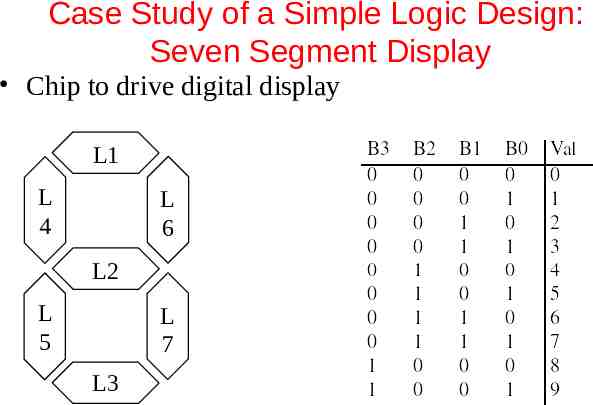
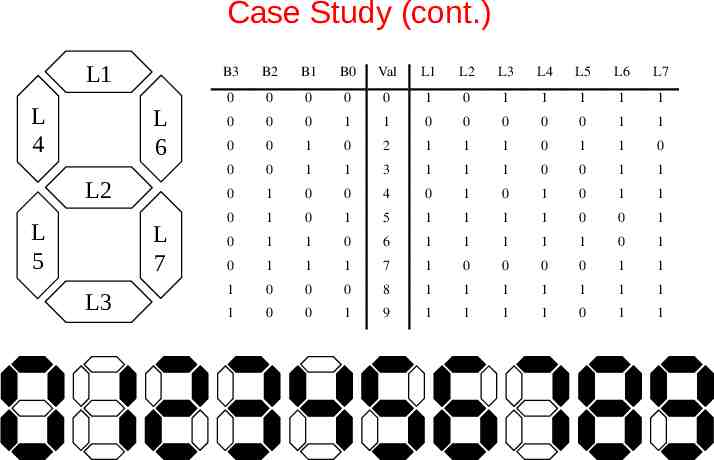
Case Study of a Simple Logic Design: Seven Segment Display Chip to drive digital display L1 L 4 L 6 L2 L 5 L 7 L3
Case Study (cont.) L1 L 4 L 6 L2 L 5 L 7 L3 B3 B2 B1 B0 Val L1 L2 L3 L4 L5 L6 L7 0 0 0 0 0 1 0 1 1 1 1 1 0 0 0 1 1 0 0 0 0 0 1 1 0 0 1 0 2 1 1 1 0 1 1 0 0 0 1 1 3 1 1 1 0 0 1 1 0 1 0 0 4 0 1 0 1 0 1 1 0 1 0 1 5 1 1 1 1 0 0 1 0 1 1 0 6 1 1 1 1 1 0 1 0 1 1 1 7 1 0 0 0 0 1 1 1 0 0 0 8 1 1 1 1 1 1 1 1 0 0 1 9 1 1 1 1 0 1 1
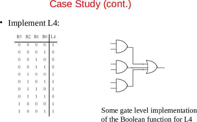
Case Study (cont.) Implement L4: Some gate level implementation of the Boolean function for L4
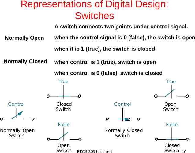
Representations of Digital Design: Switches A switch connects two points under control signal. Normally Open when the control signal is 0 (false), the switch is open when it is 1 (true), the switch is closed Normally Closed when control is 1 (true), switch is open when control is 0 (false), switch is closed True Control True Closed Switch Control False Normally Open Switch Open Switch False Normally Closed Switch Open Switch EECS 303 Lecture 1 Closed Switch 16
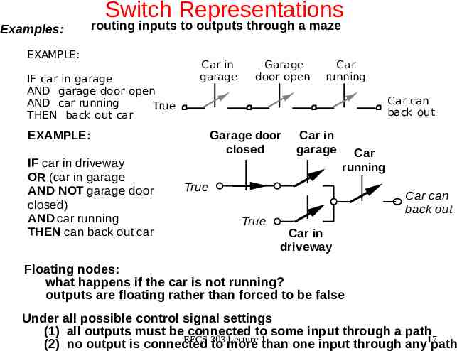
Examples: Switch Representations routing inputs to outputs through a maze EXAMPLE: IF car in garage AND garage door open AND car running True THEN back out car Car in garage Car running Car can back out EXAMPLE: IF car in driveway OR (car in garage AND NOT garage door closed) AND car running THEN can back out car Garage door open Garage door closed Car in garage Car running True True Car can back out Car in driveway Floating nodes: what happens if the car is not running? outputs are floating rather than forced to be false Under all possible control signal settings (1) all outputs must be connected to some input through a path EECS 303 Lecture 1 (2) no output is connected to more than one input through any17path
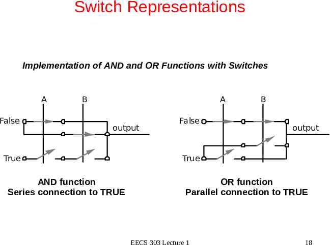
Switch Representations Implementation of AND and OR Functions with Switches A False B A output True AND function Series connection to TRUE False B output True OR function Parallel connection to TRUE EECS 303 Lecture 1 18
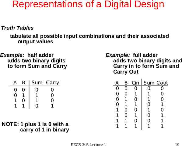
Representations of a Digital Design Truth Tables tabulate all possible input combinations and their associated output values Example: half adder adds two binary digits to form Sum and Carry A B 0 0 1 1 0 1 0 1 Example: full adder adds two binary digits and Carry in to form Sum and Carry Out Sum Carry 0 1 1 0 A 0 0 0 0 1 1 1 1 0 0 0 1 NOTE: 1 plus 1 is 0 with a carry of 1 in binary EECS 303 Lecture 1 B Cin Sum C out 0 0 0 0 0 1 1 0 1 0 1 0 1 1 0 1 0 0 1 0 0 1 0 1 1 0 0 1 1 1 1 1 19
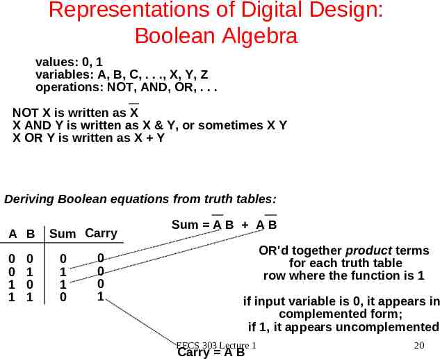
Representations of Digital Design: Boolean Algebra values: 0, 1 variables: A, B, C, . . ., X, Y, Z operations: NOT, AND, OR, . . . NOT X is written as X X AND Y is written as X & Y, or sometimes X Y X OR Y is written as X Y Deriving Boolean equations from truth tables: A B 0 0 1 1 0 1 0 1 Sum Carry 0 1 1 0 0 0 0 1 Sum A B A B OR'd together product terms for each truth table row where the function is 1 if input variable is 0, it appears in complemented form; if 1, it appears uncomplemented EECS 303 Lecture 1 Carry A B 20
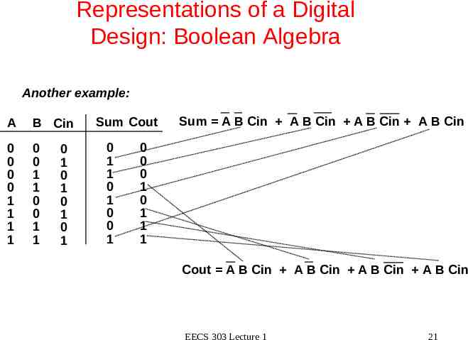
Representations of a Digital Design: Boolean Algebra Another example: A B Cin 0 0 0 0 1 1 1 1 0 0 1 1 0 0 1 1 0 1 0 1 0 1 0 1 Sum Cout 0 1 1 0 1 0 0 1 Sum A B Cin A B Cin A B Cin A B Cin 0 0 0 1 0 1 1 1 Cout A B Cin A B Cin A B Cin A B Cin EECS 303 Lecture 1 21
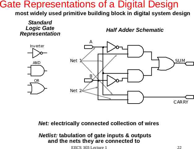
Gate Representations of a Digital Design most widely used primitive building block in digital system design Standard Logic Gate Representation Half Adder Schematic A Inverter AND Net 1 SUM B OR Net 2 CARRY Net: electrically connected collection of wires Netlist: tabulation of gate inputs & outputs and the nets they are connected to EECS 303 Lecture 1 22
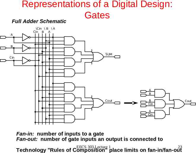
Representations of a Digital Design: Gates Full Adder Schematic A \Cin \ B \ A Cin B A B Cin SUM A B Cout B Cin Cout A Cin Fan-in: number of inputs to a gate Fan-out: number of gate inputs an output is connected to EECS 303 Lecture 1 23 Technology "Rules of Composition" place limits on fan-in/fan-out
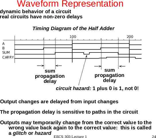
Waveform Representation dynamic behavior of a circuit real circuits have non-zero delays Timing Diagram of the Half Adder 100 200 A B SUM CARRY sum sum propagation propagation delay delay circuit hazard: 1 plus 0 is 1, not 0! Output changes are delayed from input changes The propagation delay is sensitive to paths in the circuit Outputs may temporarily change from the correct value to the wrong value back again to the correct value: this is called a glitch or hazard EECS 303 Lecture 1 24
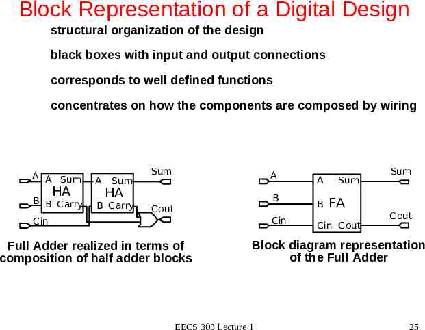
Block Representation of a Digital Design structural organization of the design black boxes with input and output connections corresponds to well defined functions concentrates on how the components are composed by wiring A A Sum A B B Carry B Carry HA Sum Sum A HA B Cout Cin Cin Full Adder realized in terms of composition of half adder blocks A B Sum FA Cin Cout Sum Cout Block diagram representation of the Full Adder EECS 303 Lecture 1 25
Introduction to Mentor Graphics Tools The Mentor Graphics CAD system has many components You will use a small portion of the tools for this course – – – – Falcon Design Framework Design Architect for entering logic designs Quicksim for simulating the designs QuickHDL for entering and simulating the VHDL designs Read through and execute Lab 1: Mentor Graphics tutorial EECS 303 Lecture 1 26
Introduction to Mentor Graphics Typing “source /vol/ece303/mgc.env” on Sun workstation will set up env for 303 labs Typing “dmgr” for Design Manager will create a window for running several tools Mentor Graphics is not a single tool but a series of design tools that uses object oriented data representation to simplify the design process Data created in one tool (e.g. design architect) can be shipped to another tool (e.g. quicksim) for simulation A schematic is merely a pictorial representation of a circuit EECS 303 Lecture 1 27
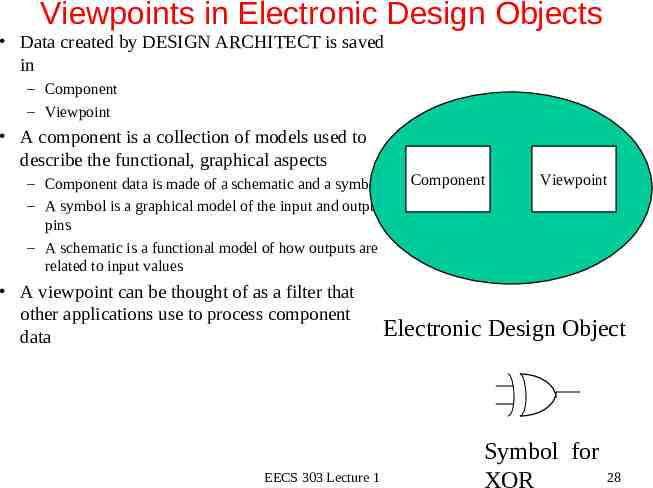
Viewpoints in Electronic Design Objects Data created by DESIGN ARCHITECT is saved in – Component – Viewpoint A component is a collection of models used to describe the functional, graphical aspects – Component data is made of a schematic and a symbol – A symbol is a graphical model of the input and output pins – A schematic is a functional model of how outputs are related to input values A viewpoint can be thought of as a filter that other applications use to process component data EECS 303 Lecture 1 Component Viewpoint Electronic Design Object Symbol for XOR 28
Moving Design Data Students familiar with UNIX, please refrain from using UNIX commands to move directories or files You MUST move these objects using the Design Manager Failure to use Design Manager will result in data corruption – Design Architect will store the absolute pathname to a design – Quicksim will try to use the symbol to look for the design from that pathname EECS 303 Lecture 1 29
Summary Class administration Digital design methodology Representations of Digital Design Introduction to Mentor Graphics tools NEXT LECTURE: Memory Elements READING: – Chapter 4 EECS 303 Lecture 1 30