Implementing PCI I/O Virtualization Standards Mike Krause and


46 Slides785.44 KB
Implementing PCI I/O Virtualization Standards Mike Krause and Renato Recio PCI SIG IOV Work Group Co-chairs
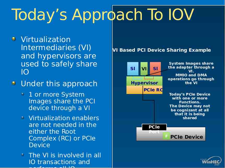
Today’s Approach To IOV Virtualization Intermediaries (VI) and hypervisors are used to safely share IO Under this approach 1 or more System Images share the PCI device through a VI Virtualization enablers are not needed in the either the Root Complex (RC) or PCIe Device The VI is involved in all IO transactions and VI Based PCI Device Sharing Example SI VI System Images share the adapter through a VI. MMIO and DMA operations go through the VI SI Hypervisor PCIe RC PCIe Port Today’s PCIe Device with one or more Functions. The Device may not be cognizant at all that it is being shared F PCIe Device
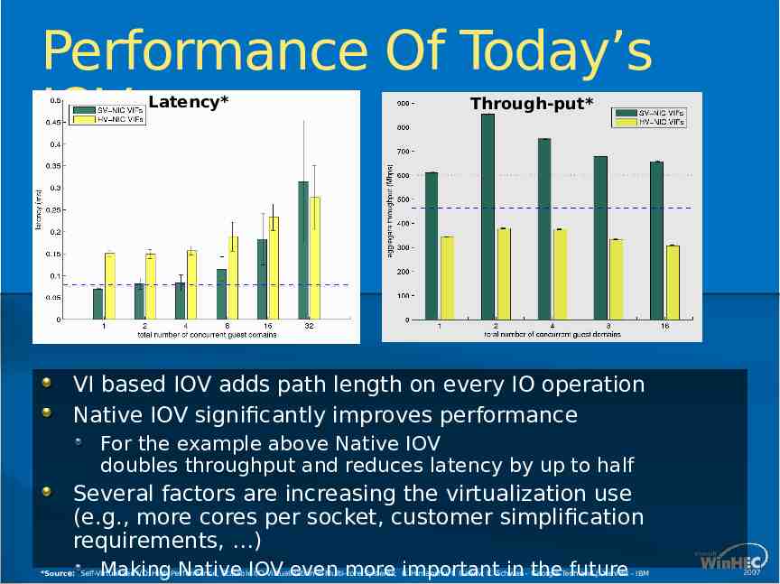
Performance Of Today’s IOV Latency* Native IOV VI Based IOV Through-put* Native IOV VI Based IOV VI based IOV adds path length on every IO operation Native IOV significantly improves performance For the example above Native IOV doubles throughput and reduces latency by up to half Several factors are increasing the virtualization use (e.g., more cores per socket, customer simplification requirements, ) Making Native IOV even more important in the future *Source: Self-Virtualized I/O: High Performance, Scalable I/O Virtualization in Multi-core Systems; R. Himanshu, I. Ganev, K. Schwan - Georgia Tech and J. Xenidis - IBM
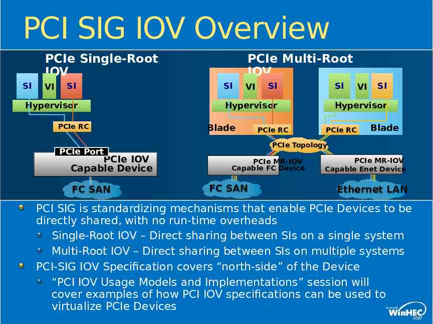
PCI SIG IOV Overview PCIe Single-Root IOV SI VI SI Hypervisor PCIe RC PCIe Multi-Root IOV SI VI FC SAN SI Hypervisor Blade PCIe RC VI SI Hypervisor PCIe RC Blade PCIe Topology PCIe Port PCIe IOV Capable Device SI PCIe MR-IOV Capable FC Device FC SAN PCIe MR-IOV Capable Enet Device Ethernet LAN PCI SIG is standardizing mechanisms that enable PCIe Devices to be directly shared, with no run-time overheads Single-Root IOV – Direct sharing between SIs on a single system Multi-Root IOV – Direct sharing between SIs on multiple systems PCI-SIG IOV Specification covers “north-side” of the Device “PCI IOV Usage Models and Implementations” session will cover examples of how PCI IOV specifications can be used to virtualize PCIe Devices
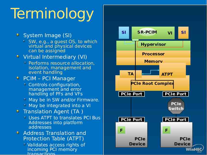
Terminology System Image (SI) SR-PCIM VI SI SW, e.g., a guest OS, to which virtual and physical devices can be assigned Hypervisor Processor Virtual Intermediary (VI) Memory Performs resource allocation, isolation, management and event handling TA PCIM – PCI Manager Controls configuration, management and error handling of PFs and VFs May be in SW and/or Firmware. May be integrated into a VI ATPT PCIe Root Complex PCIe Port PCIe Port PCIe Switch Translation Agent (TA ) Uses ATPT to translates PCI Bus Addresses into platform addresses Address Translation and Protection Table (ATPT) Validates access rights of incoming PCI memory SI VI PCIe Port PCIe Port F F PCIe Device PCIe Device
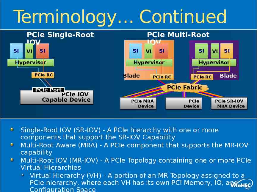
Terminology Continued PCIe Single-Root IOV SI VI SI Hypervisor PCIe RC PCIe Multi-Root IOV SI SI VI Hypervisor Blade VI SI Hypervisor PCIe RC PCIe RC Blade PCIe Fabric PCIe Port PCIe IOV Capable Device SI PCIe MRA Device PCIe Device PCIe SR-IOV MRA Device Single-Root IOV (SR-IOV) - A PCIe hierarchy with one or more components that support the SR-IOV Capability Multi-Root Aware (MRA) - A PCIe component that supports the MR-IOV capability Multi-Root IOV (MR-IOV) - A PCIe Topology containing one or more PCIe Virtual Hierarchies Virtual Hierarchy (VH) - A portion of an MR Topology assigned to a PCIe hierarchy, where each VH has its own PCI Memory, IO, and Configuration Space
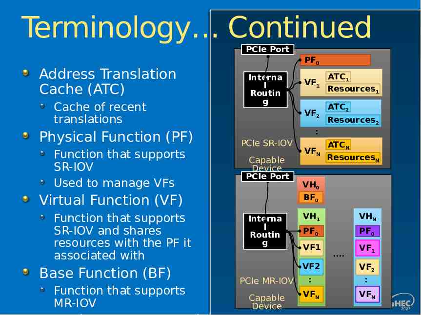
Terminology Continued PCIe Port Address Translation Cache (ATC) Cache of recent translations Physical Function (PF) Function that supports SR-IOV Used to manage VFs PF0 Interna l Routin g VF2 Base Function (BF) Function that supports MR-IOV ATC1 Resources1 ATC2 Resources2 : PCIe SR-IOV Capable Device PCIe Port Virtual Function (VF) Function that supports SR-IOV and shares resources with the PF it associated with VF1 VFN ATCN ResourcesN VH0 BF0 Interna l Routin g VH1 VHN PF0 PF0 VF1 VF1 . VF2 VF2 PCIe MR-IOV : : Capable Device VFN VFN
PCI IOV Related Mechanisms Function Level Reset (FLR) Alternative Routing ID Interpretation(ARI) Address Translation Services Single-Root IO Virtualization
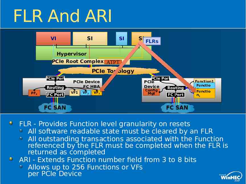
FLR And ARI SI VI SI SI FLRs Hypervisor PCIe Root Complex ATPT PCIe Topology PCIe Port Routing PF0 FC Port FC SAN PCIe Device FC HBA VF1 VF2 VF3 PCIe Port PCIe Device Config Mgt Routing FC Port Function1 Functio n2 Functio n3 FC SAN FLR - Provides Function level granularity on resets All software readable state must be cleared by an FLR All outstanding transactions associated with the Function referenced by the FLR must be completed when the FLR is returned as completed ARI - Extends Function number field from 3 to 8 bits Allows up to 256 Functions or VFs per PCIe Device
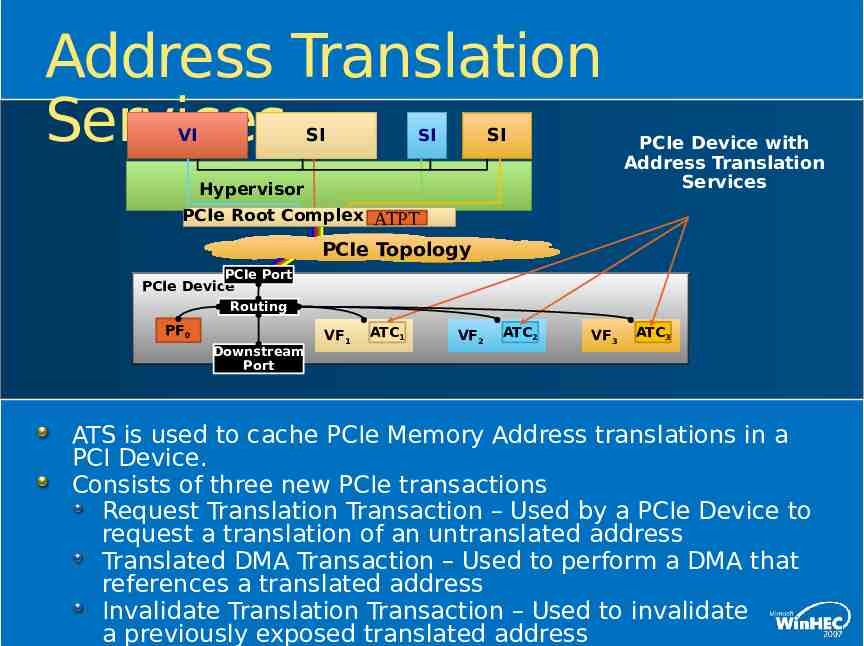
Address Translation Services SI VI SI SI Hypervisor PCIe Device with Address Translation Services PCIe Root Complex ATPT PCIe Topology PCIe Port PCIe Device Routing PF0 Downstream Port VF1 ATC1 VF2 ATC2 VF3 ATC3 ATS is used to cache PCIe Memory Address translations in a PCI Device. Consists of three new PCIe transactions Request Translation Transaction – Used by a PCIe Device to request a translation of an untranslated address Translated DMA Transaction – Used to perform a DMA that references a translated address Invalidate Translation Transaction – Used to invalidate a previously exposed translated address
PCI Single-Root IOV Overview
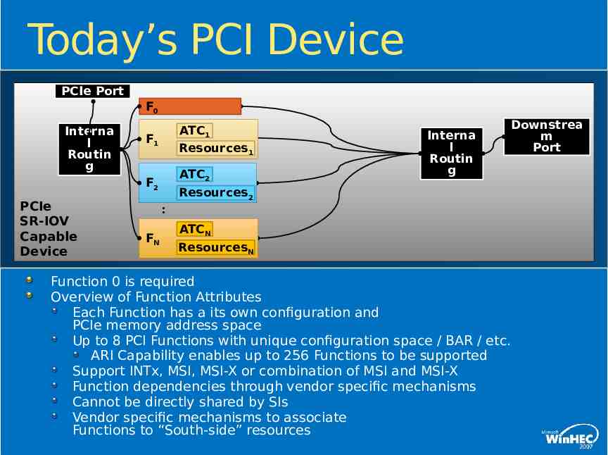
Today’s PCI Device PCIe Port F0 Interna l Routin g ATC1 Resources1 F1 ATC2 F2 PCIe SR-IOV Capable Device Interna l Routin g Downstrea m Port Resources2 : FN ATCN ResourcesN Function 0 is required Overview of Function Attributes Each Function has a its own configuration and PCIe memory address space Up to 8 PCI Functions with unique configuration space / BAR / etc. ARI Capability enables up to 256 Functions to be supported Support INTx, MSI, MSI-X or combination of MSI and MSI-X Function dependencies through vendor specific mechanisms Cannot be directly shared by SIs Vendor specific mechanisms to associate Functions to “South-side” resources
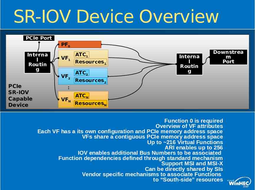
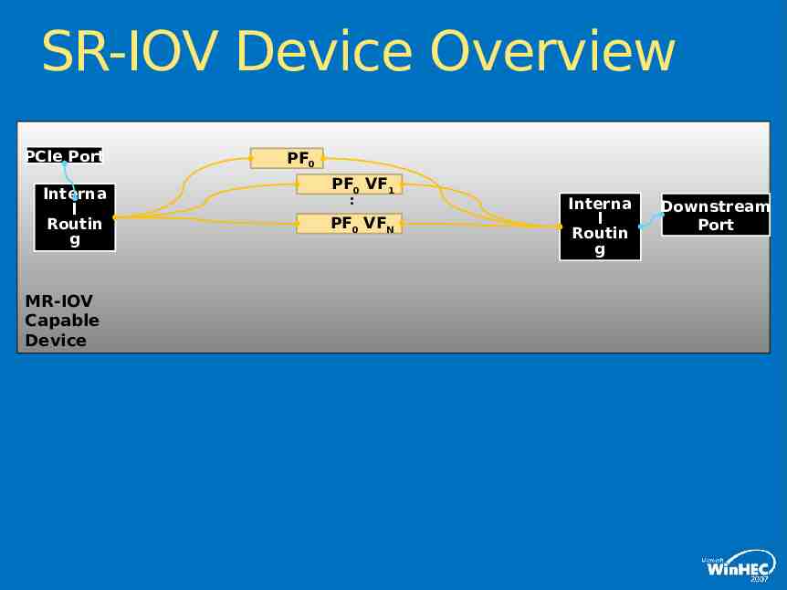
SR-IOV Device Overview PCIe Port PF0 Interna l Routin g VF1 VF2 PCIe SR-IOV Capable Device ATC1 Resources1 ATC2 Interna l Routin g Downstrea m Port Resources2 : VFN ATCN ResourcesN Function 0 is required Overview of VF attributes Each VF has a its own configuration and PCIe memory address space VFs share a contiguous PCIe memory address space Up to 216 Virtual Functions ARI enables up to 256 IOV enables additional Bus Numbers to be associated Function dependencies defined through standard mechanism Support MSI and MSI-X Can be directly shared by SIs Vendor specific mechanisms to associate Functions to “South-side” resources
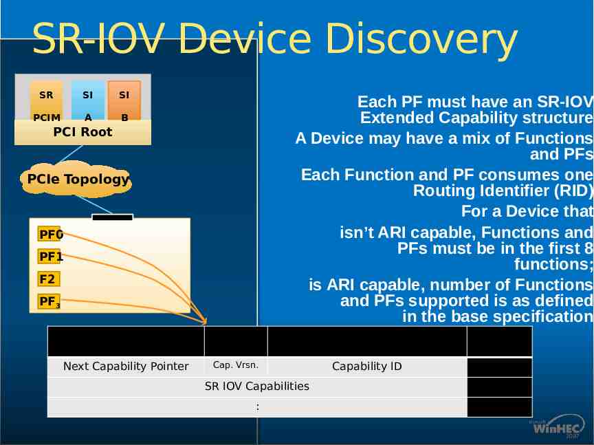
SR-IOV Device Discovery SR SI SI PCIM A B Each PF must have an SR-IOV Extended Capability structure A Device may have a mix of Functions and PFs Each Function and PF consumes one Routing Identifier (RID) For a Device that isn’t ARI capable, Functions and PFs must be in the first 8 functions; is ARI capable, number of Functions and PFs supported is as defined in the base specification PCI Root PCIe Topology PF0 PF1 F2 PF3 31 20 Next Capability Pointer 19 16 15 0 Cap. Vrsn. Offset Capability ID 00h SR IOV Capabilities 04h : :
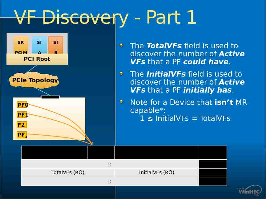
VF Discovery - Part 1 SR SI SI PCIM A B The TotalVFs field is used to discover the number of Active VFs that a PF could have. PCIe Topology The InitialVFs field is used to discover the number of Active VFs that a PF initially has. PCI Root Note for a Device that isn’t MR capable*: 1 InitialVFs TotalVFs PF0 PF1 F2 PF3 31 20 19 16 15 Offset 0 : TotalVFs (RO) : InitialVFs (RO) : 0Ch :
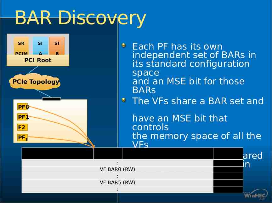
BAR Discovery SR SI SI PCIM A B Each PF has its own independent set of BARs in its standard configuration space and an MSE bit for those BARs The VFs share a BAR set and PCI Root PCIe Topology PF0 PF1 F2 PF3 31 20 have an MSE bit that controls the memory space of all the VFs 19 15 Offset 16 0 The BAR set that is shared : : by all the VFs resides in VF BAR0 (RW) 20h the PF’s SR-IOV : : VF BAR5 (RW) capabilities 34h : :
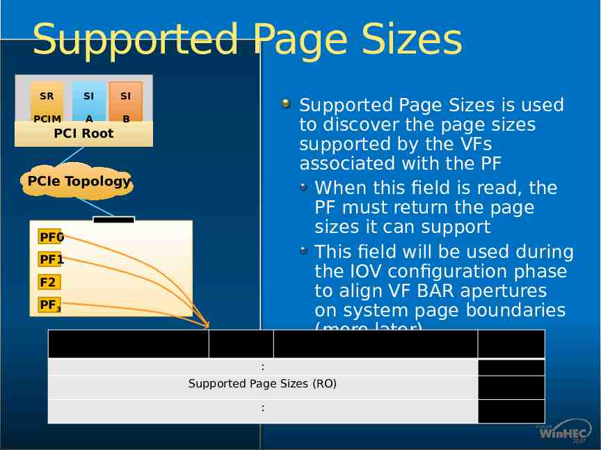
Supported Page Sizes SR SI SI PCIM A B Supported Page Sizes is used to discover the page sizes supported by the VFs associated with the PF When this field is read, the PF must return the page sizes it can support This field will be used during the IOV configuration phase to align VF BAR apertures on system page boundaries (more later) 15 Offset PCI Root PCIe Topology PF0 PF1 F2 PF3 31 20 19 16 0 : : Supported Page Sizes (RO) 18h : :
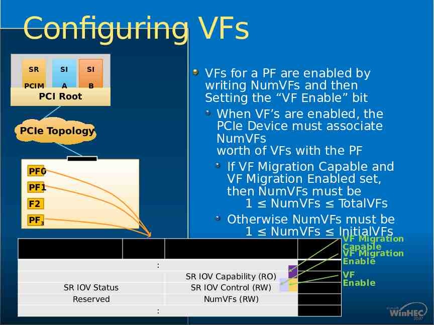
Configuring VFs SR SI SI PCIM A B VFs for a PF are enabled by writing NumVFs and then Setting the “VF Enable” bit When VF’s are enabled, the PCIe Device must associate NumVFs worth of VFs with the PF If VF Migration Capable and VF Migration Enabled set, then NumVFs must be 1 NumVFs TotalVFs Otherwise NumVFs must be 1 NumVFs InitialVFs VF Migration PCI Root PCIe Topology PF0 PF1 F2 PF3 31 20 19 16 15 0 : SR IOV Capability (RO) SR IOV Control (RW) NumVFs (RW) SR IOV Status Reserved : Offset : 04h 08h 10h : Capable VF Migration Enable VF Enable
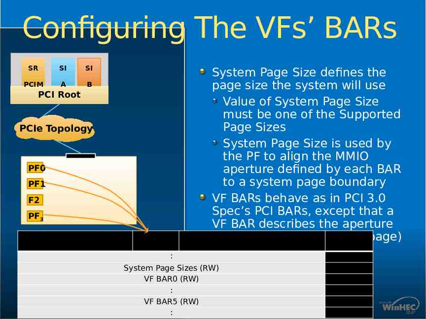
Configuring The VFs’ BARs SR SI SI PCIM A B PCI Root PCIe Topology PF0 PF1 F2 PF3 31 20 19 16 15 0 System Page Size defines the page size the system will use Value of System Page Size must be one of the Supported Page Sizes System Page Size is used by the PF to align the MMIO aperture defined by each BAR to a system page boundary VF BARs behave as in PCI 3.0 Spec’s PCI BARs, except that a VF BAR describes the aperture for multiple VFs (see Offset next page) : System Page Sizes (RW) VF BAR0 (RW) : VF BAR5 (RW) : : 1Ch 20h : 34h :
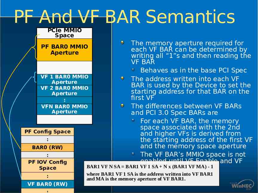
PF And VF BAR Semantics PCIe MMIO Space The memory aperture required for each VF BAR can be determined by writing all “1”s and then reading the VF BAR Behaves as in the base PCI Spec VF 1 BAR0 MMIO The address written into each VF Aperture BAR is used by the Device to set the VF 2 BAR0 MMIO starting address for that BAR on the Aperture first VF : VFN BAR0 MMIO The differences between VF BARs Aperture and PCI 3.0 Spec BARs are For each VF BAR, the memory space associated with the 2nd PF Config Space and higher VFs is derived from : the starting address of the first VF and the memory space aperture BAR0 (RW) The VF BAR’s MMIO space is not : enabled until VF Enable and VF PF IOV Config BAR1 VF N SA BAR1 VF 1 SAhave N x (BAR1 MA) - 1 MSE beenVFset Space PF BAR0 MMIO Aperture : VF BAR0 (RW) where BAR1 VF 1 SA is the address written into VF BAR1 and MA is the memory aperture of VF BAR1.
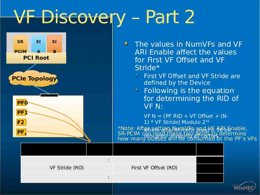
VF Discovery – Part 2 SR SI SI PCIM A B The values in NumVFs and VF ARI Enable affect the values for First VF Offset and VF Stride* PCI Root First VF Offset and VF Stride are defined by the Device PCIe Topology Following is the equation for determining the RID of VF N: PF0 PF1 VF N [PF RID VF Offset (N1) * VF Stride] Modulo 216 F2 *Note: After setting NumVFs and ARIbit Enable, where all arithmetic usedVF is 16 SR-PCIM can read these twoall fields to determine unsigned dropping carries how many busses will be consumed bt the PF’s VFs PF3 31 20 19 16 15 Offset 0 : VF Stride (RO) : First VF Offset (RO) : 14h :
PF And VF BAR Semantics PF 0 RID 0200 PF 0 IOV Config Space : Reserv ed NumVFs 0050x VF VF Stride Offset 0002x 0004x PF 1 RID 0201 : PF 1 IOV Config Space : Reserv ed NumVFs 0003x VF Stride 0004x VF Offset 0002x : PCIe RID Number RID Func. # : : 020 PF 0 0 020 PF 1 1 020 VF 0,1 2 020 VF 1,1 3 020 4 020 5 020 VF 0,2 6 020 VF 1,2 7 020 8 020 9 020 VF 0,3 A 020 PF and VF RIDs must not overlap given any valid NumVFs setting across all PFs of a Device As in base, an SR-IOV Device captures Bus # from any Type 0 config request VFs may reside on a different bus number as associated PF If the switch above the Device supports ARI Forwarding bit, RIDs are interpreted as 8 bit Bus # and 8 bit Device # doesn’t supports ARI, RIDs are interpreted as BDF# Bus # can be used to assign VFs, but PFs must be on 1st
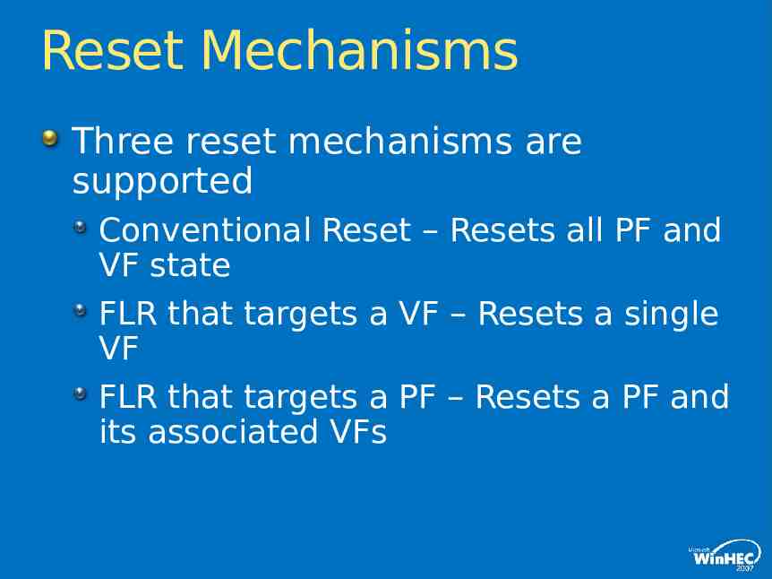
Reset Mechanisms Three reset mechanisms are supported Conventional Reset – Resets all PF and VF state FLR that targets a VF – Resets a single VF FLR that targets a PF – Resets a PF and its associated VFs
Conventional Reset A Fundamental or Hot Reset to an SR-IOV Device shall cause all Functions, PFs, and VFs context to be reset to their original, power-on state If a PF has its VFs enabled and a Fundamental or Hot Reset is issued to the Device, the Device must reset all PF and VF state, eg: The PF must disable its SR-IOV capabilities and reverts back to being a PCI Function Settable SR-IOV capabilities (e.g., NumVFs) are reset to default values MSE and BME are both off
FLRs To VFs And PFs An FLR that targets a VF must be supported Software may use FLR to reset a VF An FLR that targets a VF must Not affect the VFs existence (e.g. it still consumes a RID) Not affect any address assigned to it. That is, the VF’s BAR registers and MSE are unaffected by FLR An FLR that targets a PF must be supported Software may use an FLR to reset a PF An FLR that targets a PF must
PCI Multi-Root IOV Overview
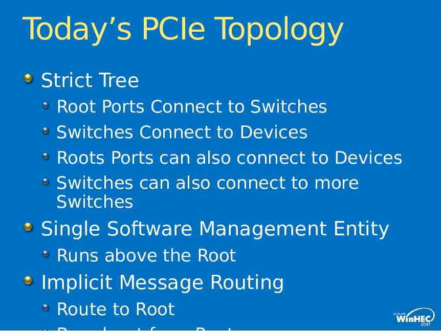
Today’s PCIe Topology Strict Tree Root Ports Connect to Switches Switches Connect to Devices Roots Ports can also connect to Devices Switches can also connect to more Switches Single Software Management Entity Runs above the Root Implicit Message Routing Route to Root
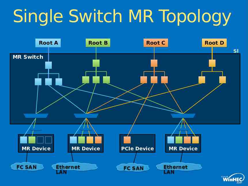
Single Switch MR Topology Root B Root A Root C Root D SI MR Switch MR Device FC SAN MR Device Ethernet LAN PCIe Device FC SAN MR Device Ethernet LAN
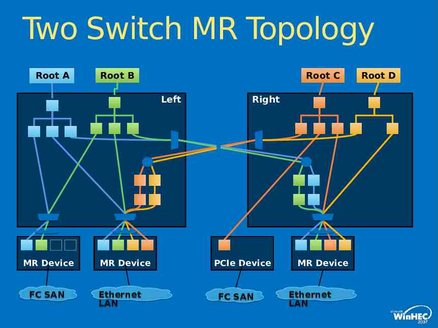
Two Switch MR Topology Root A Root B Root C Left MR Device FC SAN MR Device Ethernet LAN Right PCIe Device FC SAN MR Device Ethernet LAN Root D
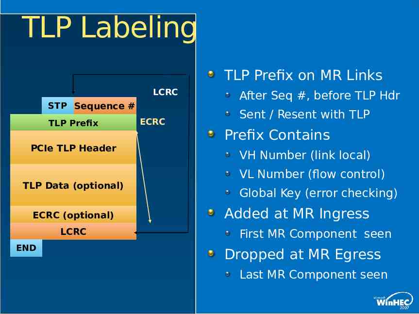
TLP Labeling TLP Prefix on MR Links LCRC STP Sequence # TLP Prefix PCIe TLP Header TLP Data (optional) ECRC (optional) LCRC END ECRC After Seq #, before TLP Hdr Sent / Resent with TLP Prefix Contains VH Number (link local) VL Number (flow control) Global Key (error checking) Added at MR Ingress First MR Component seen Dropped at MR Egress Last MR Component seen
SR-IOV Device Overview PCIe Port Interna l Routin g MR-IOV Capable Device PF0 PF0 VF1 : PF0 VFN Interna l Routin g Downstream Port
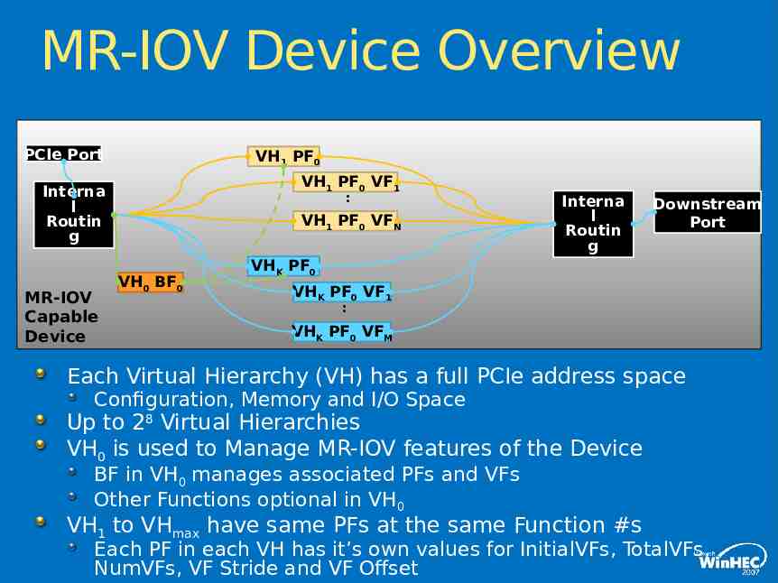
MR-IOV Device Overview PCIe Port VH1 PF0 VH1 PF0 VF1 Interna l Routin g MR-IOV Capable Device : VH1 PF0 VFN VH0 BF0 Interna l Routin g Downstream Port VHK PF0 VHK PF0 VF1 : VHK PF0 VFM Each Virtual Hierarchy (VH) has a full PCIe address space Configuration, Memory and I/O Space Up to 28 Virtual Hierarchies VH0 is used to Manage MR-IOV features of the Device BF in VH0 manages associated PFs and VFs Other Functions optional in VH0 VH1 to VHmax have same PFs at the same Function #s Each PF in each VH has it’s own values for InitialVFs, TotalVFs, NumVFs, VF Stride and VF Offset
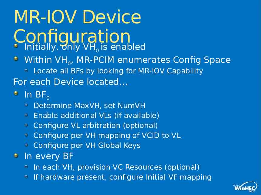
MR-IOV Device Configuration Initially, only VH is enabled 0 Within VH0, MR-PCIM enumerates Config Space Locate all BFs by looking for MR-IOV Capability For each Device located In BF0 Determine MaxVH, set NumVH Enable additional VLs (if available) Configure VL arbitration (optional) Configure per VH mapping of VCID to VL Configure per VH Global Keys In every BF In each VH, provision VC Resources (optional) If hardware present, configure Initial VF mapping
PCI Specification Schedule ATS SR-IOV MR-IOV
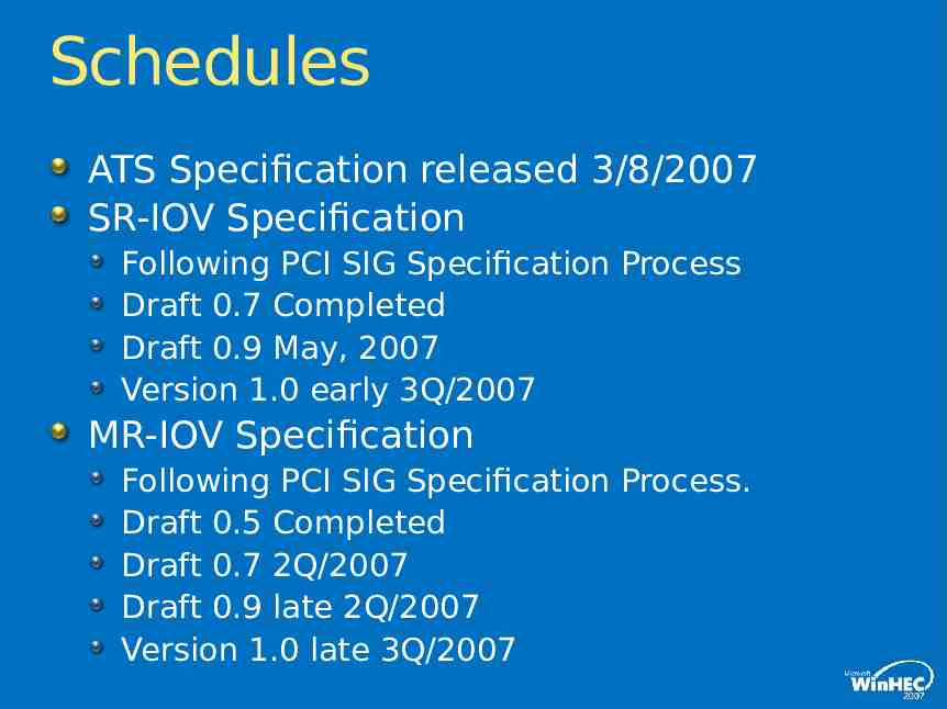
Schedules ATS Specification released 3/8/2007 SR-IOV Specification Following PCI SIG Specification Process Draft 0.7 Completed Draft 0.9 May, 2007 Version 1.0 early 3Q/2007 MR-IOV Specification Following PCI SIG Specification Process. Draft 0.5 Completed Draft 0.7 2Q/2007 Draft 0.9 late 2Q/2007 Version 1.0 late 3Q/2007
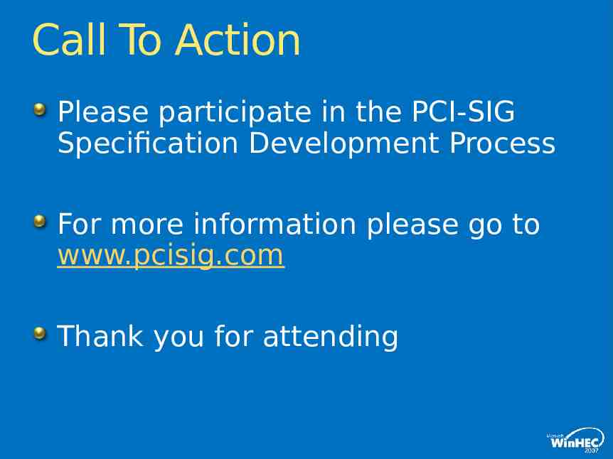
Call To Action Please participate in the PCI-SIG Specification Development Process For more information please go to www.pcisig.com Thank you for attending
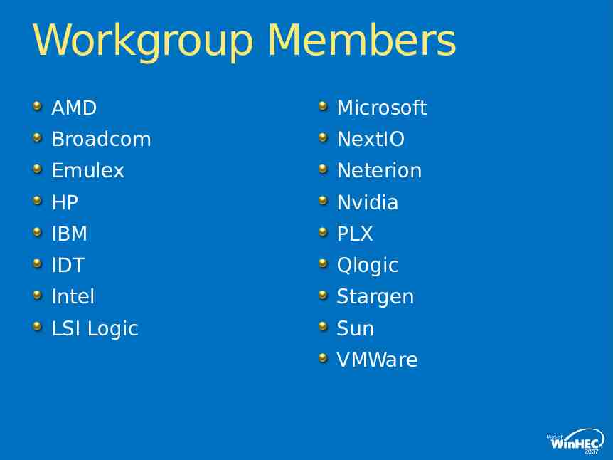
Workgroup Members AMD Microsoft Broadcom NextIO Emulex Neterion HP Nvidia IBM PLX IDT Qlogic Intel Stargen LSI Logic Sun VMWare
Question s
MR Topics Back-ups
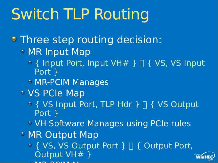
Switch TLP Routing Three step routing decision: MR Input Map { Input Port, Input VH# } { VS, VS Input Port } MR-PCIM Manages VS PCIe Map { VS Input Port, TLP Hdr } { VS Output Port } VH Software Manages using PCIe rules MR Output Map { VS, VS Output Port } { Output Port, Output VH# }
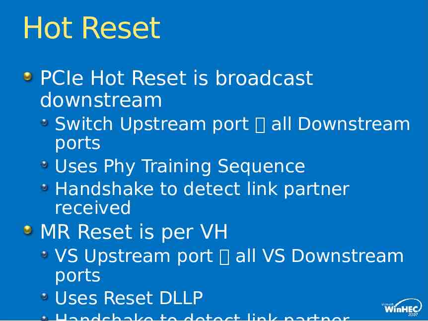
Hot Reset PCIe Hot Reset is broadcast downstream Switch Upstream port all Downstream ports Uses Phy Training Sequence Handshake to detect link partner received MR Reset is per VH VS Upstream port all VS Downstream ports Uses Reset DLLP
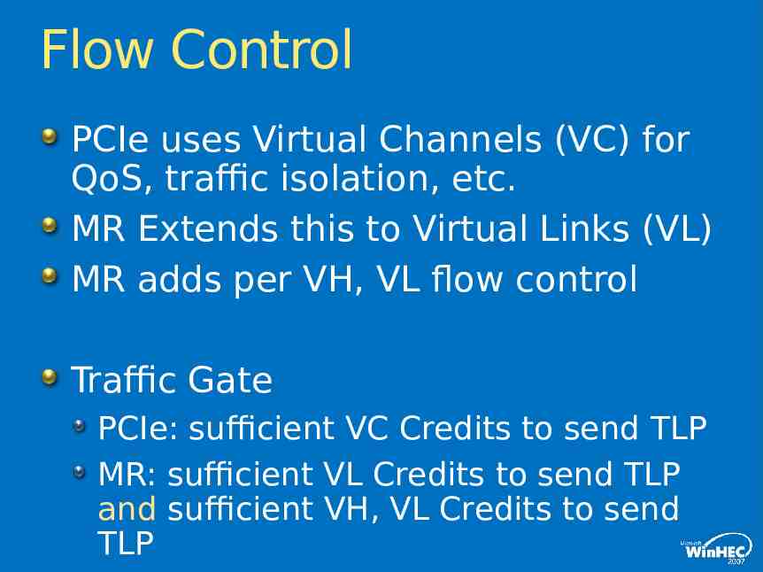
Flow Control PCIe uses Virtual Channels (VC) for QoS, traffic isolation, etc. MR Extends this to Virtual Links (VL) MR adds per VH, VL flow control Traffic Gate PCIe: sufficient VC Credits to send TLP MR: sufficient VL Credits to send TLP and sufficient VH, VL Credits to send TLP
Management / Authorization Devices are managed using VH0 Switches are managed using the Upstream port of any Authorized VS Multiple VS may be simultaneously authorized Supports MR-PCIM failover At failover, new MR-PCIM remaps VH0 so it can mange MR Devices
Virtual Hot Plug Virtual Hot Plug is implemented in each Downstream Port of each VS Software in VH sees PCIe Slot Control Regs MR-PCIM controls virtual “buttons & lights” e.g. pushing the virtual Attention Button, detecting virtual slot power state, Physical Hot-Plug is implemented in each Physical Port Managed by MR-PCIM Optional (same as PCIe)
Power Management Each PF has a power state if all PFs in low power state, link can go to low power state (like PCIe multifunction rules) PM PME Messages sometimes trigger WAKE# e.g., some Root powered itself off but a shared device below it was only virtually powered off (Device still being used by other VHs)
2007 Microsoft Corporation. All rights reserved. Microsoft, Windows, Windows Vista and other product names are or may be registered trademarks and/or trademarks in the U.S. and/or other countries. The information herein is for informational purposes only and represents the current view of Microsoft Corporation as of the date of this presentation. Because Microsoft must respond to changing market conditions, it should not be interpreted to be a commitment on the part of Microsoft, and Microsoft cannot guarantee the accuracy of any information provided after the date of this presentation. MICROSOFT MAKES NO WARRANTIES, EXPRESS, IMPLIED OR STATUTORY, AS TO THE INFORMATION IN THIS PRESENTATION.