CS4100: 計算機結構 Designing a Single-Cycle Processor


67 Slides1.35 MB
CS4100: 計算機結構 Designing a Single-Cycle Processor 國立清華大學資訊工程學系 一零零學年度第二學期
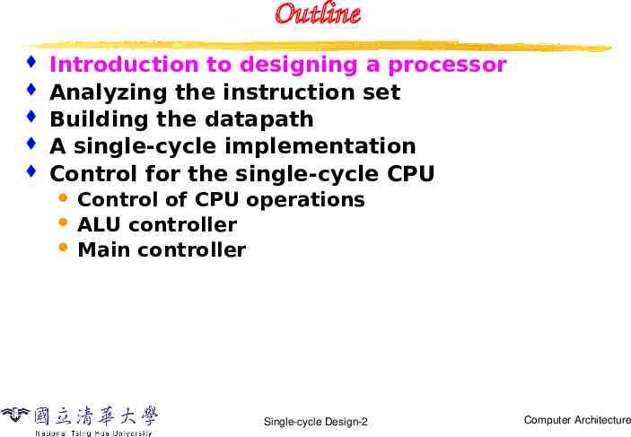
Outline Introduction to designing a processor Analyzing the instruction set Building the datapath A single-cycle implementation Control for the single-cycle CPU Control of CPU operations ALU controller Main controller Single-cycle Design-2 Computer Architecture
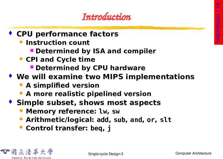
§4.1 Introduction Introduction CPU performance factors Instruction count Determined by ISA and compiler CPI and Cycle time Determined by CPU hardware We will examine two MIPS implementations A simplified version A more realistic pipelined version Simple subset, shows most aspects Memory reference: lw, sw Arithmetic/logical: add, sub, and, or, slt Control transfer: beq, j Single-cycle Design-3 Computer Architecture
Instruction Execution PC instruction memory, fetch instruction Register numbers register file, read registers Depending on instruction class Use ALU to calculate Arithmetic result Memory address for load/store Branch target address Access data memory for load/store PC target address or PC 4 Single-cycle Design-4 Computer Architecture
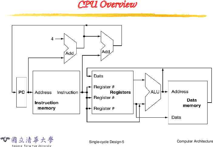
CPU Overview Single-cycle Design-5 Computer Architecture
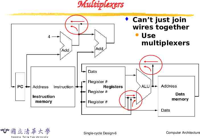
Multiplexers Single-cycle Design-6 Can’t just join wires together Use multiplexers Computer Architecture
Control Single-cycle Design-7 Computer Architecture
Information encoded in binary Low voltage 0, High voltage 1 One wire per bit Multi-bit data encoded on multi-wire buses Combinational element Operate on data Output is a function of input State (sequential) elements Store information Single-cycle Design-8 Computer Architecture §4.2 Logic Design Conventions Logic Design Basics
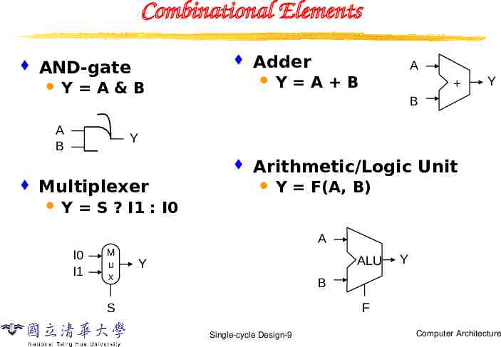
Combinational Elements AND-gate Y A&B A B Y A B Y Y Multiplexer A B Adder Arithmetic/Logic Unit Y F(A, B) Y S ? I1 : I0 A I0 I1 M u x ALU Y Y B F S Single-cycle Design-9 Computer Architecture
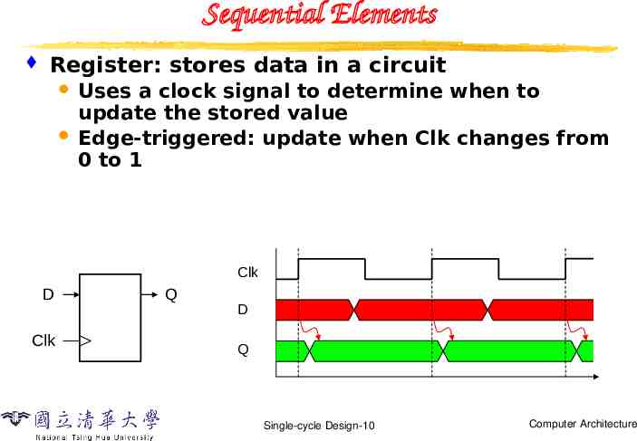
Sequential Elements Register: stores data in a circuit Uses a clock signal to determine when to update the stored value Edge-triggered: update when Clk changes from 0 to 1 Clk D Clk Q D Q Single-cycle Design-10 Computer Architecture
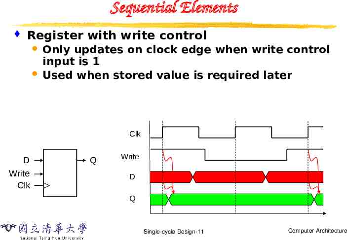
Sequential Elements Register with write control Only updates on clock edge when write control input is 1 Used when stored value is required later Clk D Write Clk Q Write D Q Single-cycle Design-11 Computer Architecture
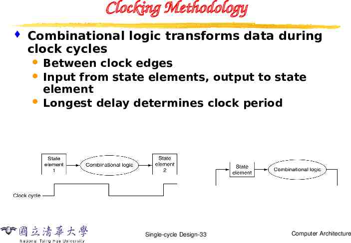
Clocking Methodology Combinational logic transforms data during clock cycles Between clock edges Input from state elements, output to state element Longest delay determines clock period Single-cycle Design-12 Computer Architecture
How to Design a Processor? 1. Analyze instruction set (datapath requirements) The meaning of each instruction is given by the register transfers Datapath must include storage element Datapath must support each register transfer 2. Select set of datapath components and establish clocking methodology 3. Assemble datapath meeting the requirements 4. Analyze implementation of each instruction to determine setting of control points effecting register transfer 5. Assemble the control logic Single-cycle Design-13 Computer Architecture
Outline Introduction to designing a processor Analyzing the instruction set (step 1) Building the datapath A single-cycle implementation Control for the single-cycle CPU Control of CPU operations ALU controller Main controller Single-cycle Design-14 Computer Architecture
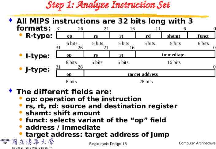
Step 1: Analyze Instruction Set All MIPS instructions are 32 bits long with 3 26 21 16 11 6 formats: 31 R-type: 31 I-type: J-type: op rs rt 6 bits 5 bits 5 bits 26 op 31 6 bits 21 rs 26 5 bits 16 5 bits 5 bits op shamt funct 5 bits 6 bits 0 immediate rt 16 bits 0 target address 6 bits rd 0 26 bits The different fields are: op: operation of the instruction rs, rt, rd: source and destination register shamt: shift amount funct: selects variant of the “op” field address / immediate target address: target address of jump Single-cycle Design-15 Computer Architecture
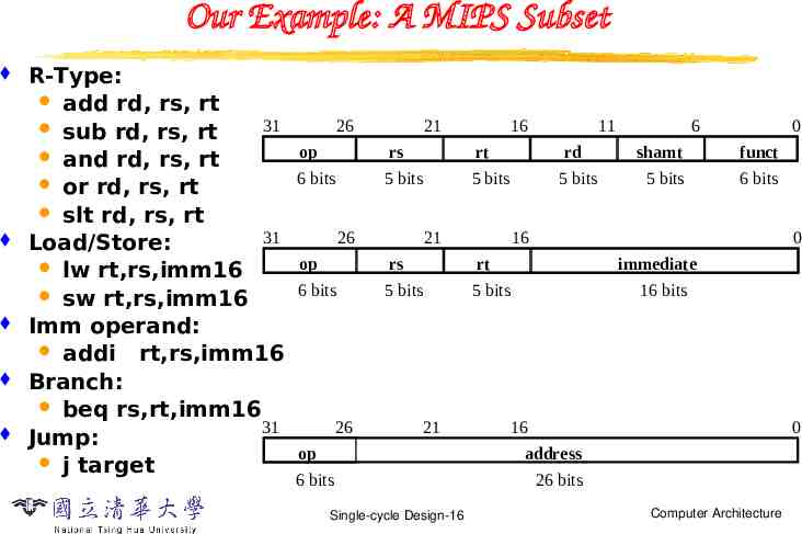
Our Example: A MIPS Subset R-Type: add rd, rs, rt 31 sub rd, rs, rt and rd, rs, rt or rd, rs, rt slt rd, rs, rt 31 Load/Store: lw rt,rs,imm16 sw rt,rs,imm16 Imm operand: addi rt,rs,imm16 Branch: beq rs,rt,imm16 31 Jump: j target 26 21 16 op rs rt 6 bits 5 bits 5 bits 26 rd 21 rs rt 6 bits 5 bits 5 bits 21 op 5 bits 6 0 shamt funct 5 bits 6 bits 16 op 26 11 0 immediate 16 bits 16 0 address 6 bits Single-cycle Design-16 26 bits Computer Architecture
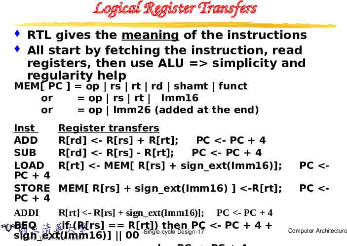
Logical Register Transfers RTL gives the meaning of the instructions All start by fetching the instruction, read registers, then use ALU simplicity and regularity help MEM[ PC ] op rs rt rd shamt funct or op rs rt Imm16 or op Imm26 (added at the end) Inst Register transfers ADD R[rd] - R[rs] R[rt]; PC - PC 4 SUB R[rd] - R[rs] - R[rt]; PC - PC 4 LOAD R[rt] - MEM[ R[rs] sign ext(Imm16)]; PC 4 STORE MEM[ R[rs] sign ext(Imm16) ] -R[rt]; PC 4 ADDI R[rt] - R[rs] sign ext(Imm16)]; PC - PC 4 BEQ if (R[rs] R[rt]) then PC - PC 4 Single-cycle Design-17 sign ext(Imm16)] 00 PC PC - Computer Architecture
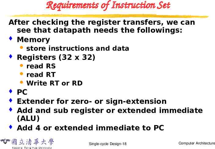
Requirements of Instruction Set After checking the register transfers, we can see that datapath needs the followings: Memory store instructions and data Registers (32 x 32) read RS read RT Write RT or RD PC Extender for zero- or sign-extension Add and sub register or extended immediate (ALU) Add 4 or extended immediate to PC Single-cycle Design-18 Computer Architecture
Outline Introduction to designing a processor Analyzing the instruction set Building the datapath (steps 2, 3) A single-cycle implementation Control for the single-cycle CPU Control of CPU operations ALU controller Main controller Single-cycle Design-19 Computer Architecture
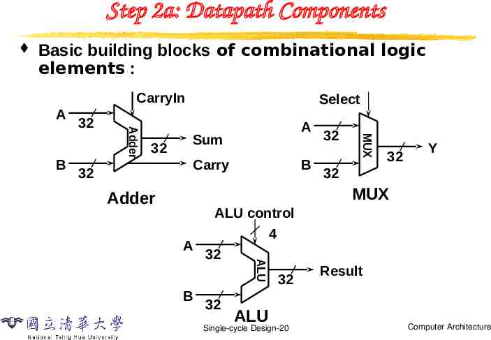
Step 2a: Datapath Components Basic building blocks of combinational logic elements : CarryIn A 32 Sum Carry 32 Adder A B 32 MUX Adder B 32 Select 32 Y 32 MUX ALU ALU control 4 A 32 B 32 ALU 32 Single-cycle Design-20 Result Computer Architecture
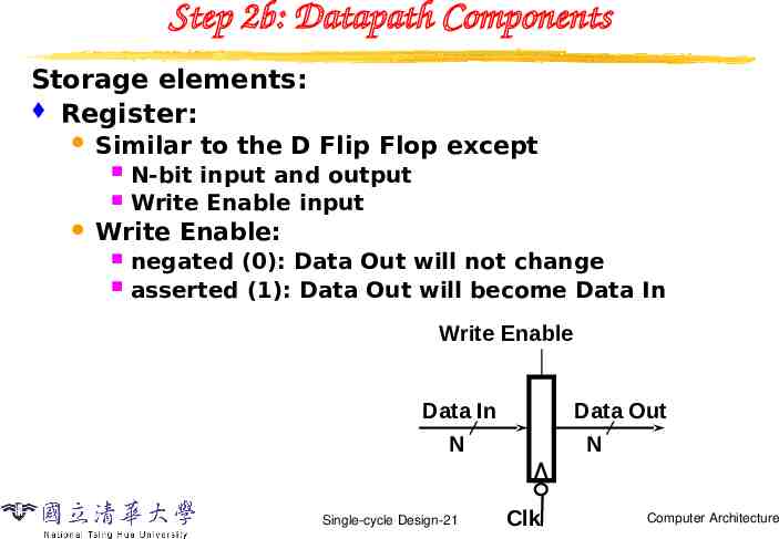
Step 2b: Datapath Components Storage elements: Register: Similar to the D Flip Flop except N-bit input and output Write Enable input Write Enable: negated (0): Data Out will not change asserted (1): Data Out will become Data In Write Enable Data In N Single-cycle Design-21 Data Out N Clk Computer Architecture
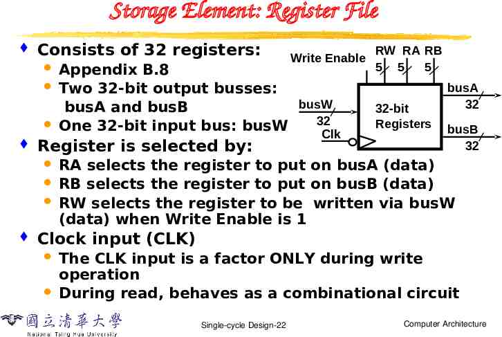
Storage Element: Register File Consists of 32 registers: Appendix B.8 Two 32-bit output busses: busW busA and busB 32 One 32-bit input bus: busW Clk Write Enable Register is selected by: RW RA RB 5 5 5 32-bit Registers busA 32 busB 32 RA selects the register to put on busA (data) RB selects the register to put on busB (data) RW selects the register to be written via busW (data) when Write Enable is 1 Clock input (CLK) The CLK input is a factor ONLY during write operation During read, behaves as a combinational circuit Single-cycle Design-22 Computer Architecture
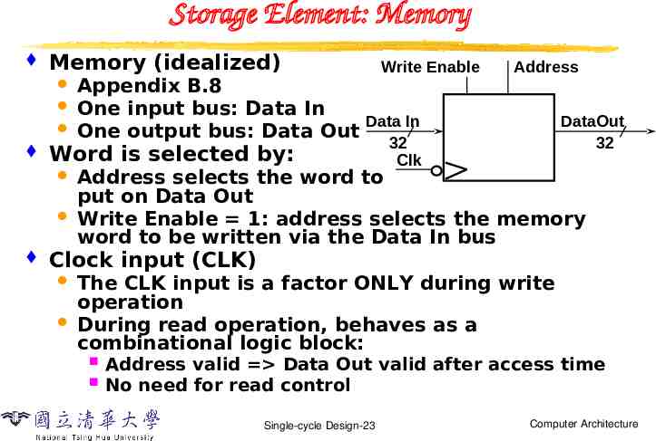
Storage Element: Memory Memory (idealized) Write Enable Appendix B.8 One input bus: Data In One output bus: Data Out Data In Address Word is selected by: DataOut 32 32 Clk Address selects the word to put on Data Out Write Enable 1: address selects the memory word to be written via the Data In bus Clock input (CLK) The CLK input is a factor ONLY during write operation During read operation, behaves as a combinational logic block: Address valid Data Out valid after access time No need for read control Single-cycle Design-23 Computer Architecture
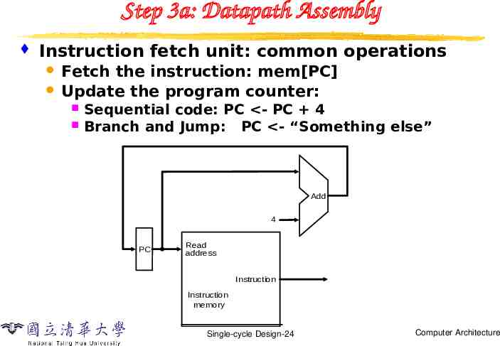
Step 3a: Datapath Assembly Instruction fetch unit: common operations Fetch the instruction: mem[PC] Update the program counter: Sequential code: PC - PC 4 Branch and Jump: PC - “Something else” Add 4 PC Read address Instruction Instruction memory Single-cycle Design-24 Computer Architecture
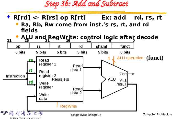
Step 3b: Add and Subtract R[rd] - R[rs] op R[rt] Ex: add rd, rs, rt Ra, Rb, Rw come from inst.’s rs, rt, and rd fields ALU and RegWrite: control logic after decode 26 21 16 11 6 0 31 op rs rt 6 bits 5 bits 5 bits rs rt Instruction rd 5 bits shamt funct 5 bits 4 Read register 1 Read register 2 Registers Write register Write data rd Read data 1 6 bits ALU operation (funct) Zero ALU ALU result Read data 2 RegWrite Single-cycle Design-25 Computer Architecture
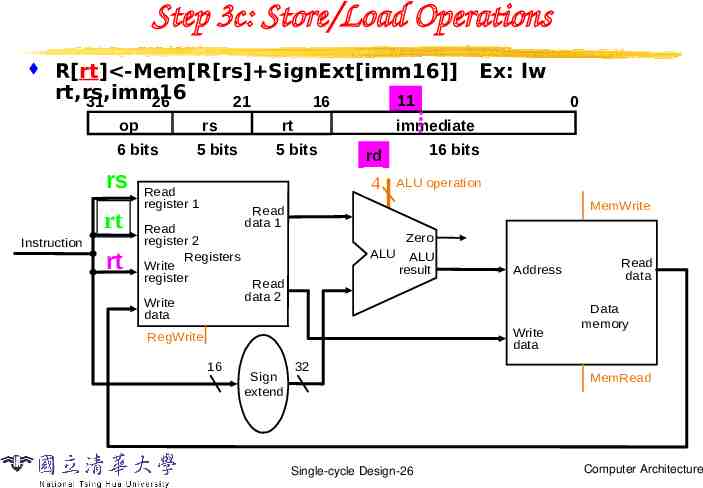
Step 3c: Store/Load Operations R[rt] -Mem[R[rs] SignExt[imm16]] rt,rs,imm16 11 31 26 21 16 op 6 bits rs rt Instruction rt rs 5 bits rt 5 bits Read register 2 Registers Write register Write data 0 immediate 16 bits rd 43 Read register 1 Ex: lw ALU operation MemWrite Read data 1 Zero ALU ALU result Address Read data 2 Write data RegWrite 16 Sign extend 32 Single-cycle Design-26 Read data Data memory MemRead Computer Architecture
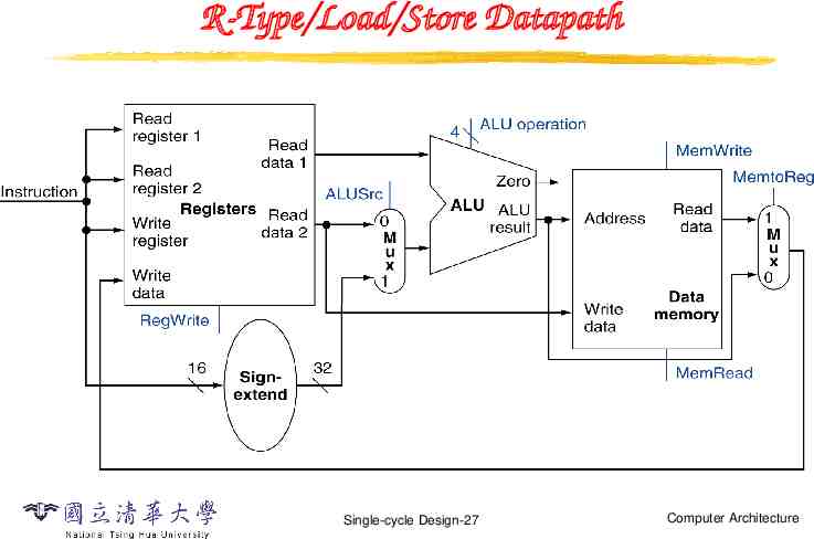
R-Type/Load/Store Datapath Single-cycle Design-27 Computer Architecture
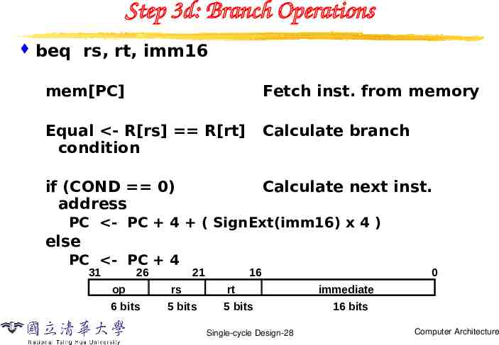
Step 3d: Branch Operations beq rs, rt, imm16 mem[PC] Fetch inst. from memory Equal - R[rs] R[rt] condition Calculate branch if (COND 0) address Calculate next inst. PC - PC 4 ( SignExt(imm16) x 4 ) else PC - PC 4 31 26 op 6 bits 21 rs 5 bits 16 rt 5 bits Single-cycle Design-28 0 immediate 16 bits Computer Architecture
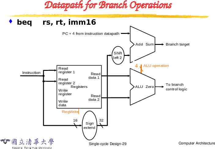
Datapath for Branch Operations beq rs, rt, imm16 PC 4 from instruction datapath Add Sum Branch target Shift left 2 Instruction 43 Read register 1 Read register 2 Registers Write register Write data ALU operation Read data 1 ALU Zero To branch control logic Read data 2 RegWrite 16 Sign extend 32 Single-cycle Design-29 Computer Architecture
Outline Introduction to designing a processor Analyzing the instruction set Building the datapath A single-cycle implementation Control for the single-cycle CPU Control of CPU operations ALU controller Main controller Single-cycle Design-30 Computer Architecture
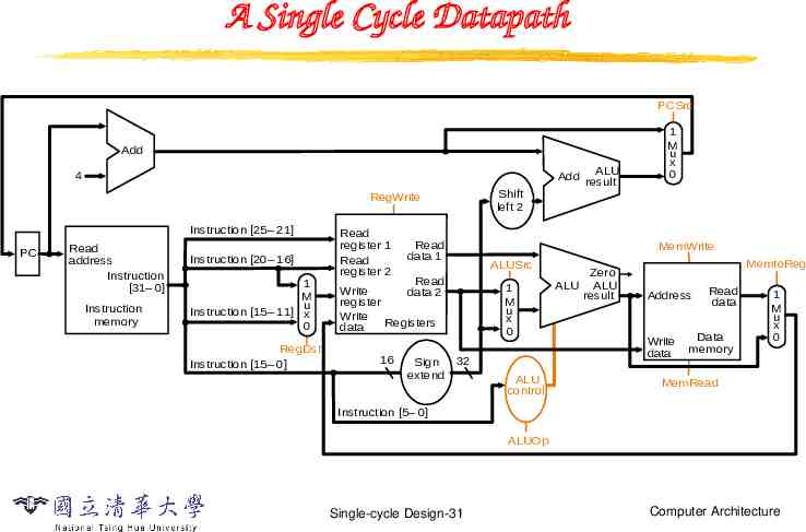
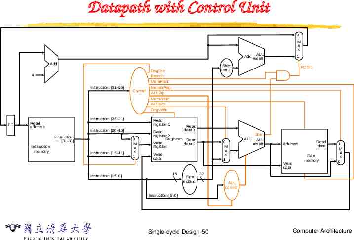
A Single Cycle Datapath PCSrc Add 4 Shift left 2 RegWrite Instruction [25– 21] PC Read address Instruction [31– 0] Instruction memory Instruction [20– 16] 1 M u Instruction [15– 11] x 0 RegDst Instruction [15– 0] Read register 1 Read register 2 Read data 1 MemWrite ALUSrc Read Write data 2 register Write Registers data 16 Sign extend ALU Add result 1 M u x 0 1 M u x 0 32 ALU control Zero ALU ALU result MemtoReg Address Write data Read data Data memory 1 M u x 0 MemRead Instruction [5– 0] ALUOp Single-cycle Design-31 Computer Architecture
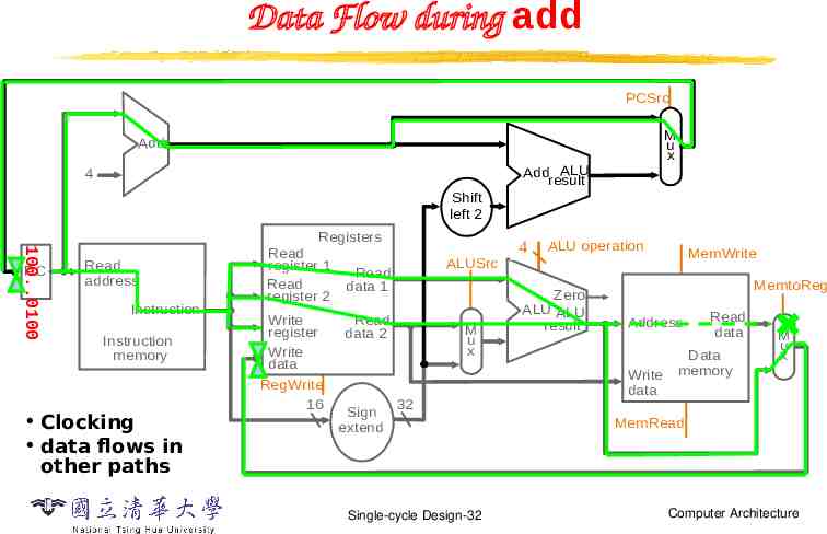
Data Flow during add PCSrc M u x Add Add ALU result 4 Shift left 2 100.0100 PC Read address Instruction Instruction memory Clocking data flows in other paths Registers Read register 1 Read Read data 1 register 2 Write register Write data RegWrite 16 ALUSrc Read data 2 Sign extend M u x 32 Single-cycle Design-32 43 ALU operation Zero ALU ALU result MemWrite MemtoReg Address Write data Read data Data memory M u x MemRead Computer Architecture
Clocking Methodology Combinational logic transforms data during clock cycles Between clock edges Input from state elements, output to state element Longest delay determines clock period Single-cycle Design-33 Computer Architecture
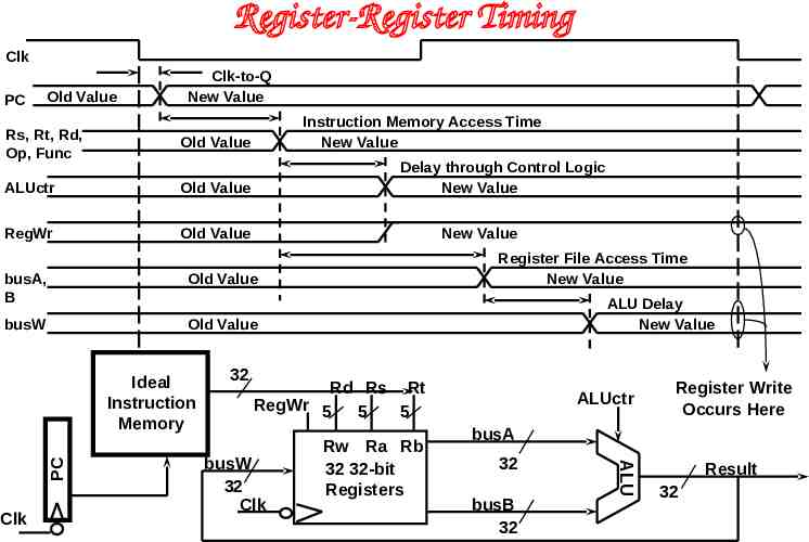
Register-Register Timing Clk PC Old Value Clk-to-Q New Value Rs, Rt, Rd, Op, Func Old Value ALUctr Old Value RegWr Old Value Instruction Memory Access Time New Value Delay through Control Logic New Value New Value busA, B Old Value busW Old Value Clk 32 ALU Delay New Value Rd Rs Rt RegWr 5 5 5 busW 32 Clk Rw Ra Rb 32 32-bit Registers ALUctr Register Write Occurs Here busA 32 busB 32 ALU PC Ideal Instruction Memory Register File Access Time New Value Result 32
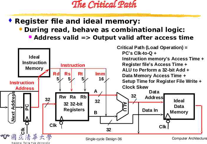
The Critical Path Register file and ideal memory: During read, behave as combinational logic: Address valid Output valid after access time Ideal Instruction Memory Instruction Rd 5 Instruction Address Rt 5 Imm 16 A PC 32 Clk Rs 5 Clk Rw Ra Rb 32 32-bit Registers 32 ALU Next Address Critical Path (Load Operation) PC’s Clk-to-Q Instruction memory’s Access Time Register file’s Access Time ALU to Perform a 32-bit Add Data Memory Access Time Setup Time for Register File Write Clock Skew Data 32 Address Ideal Data Data In Memory B 32 Single-cycle Design-36 Clk Computer Architecture
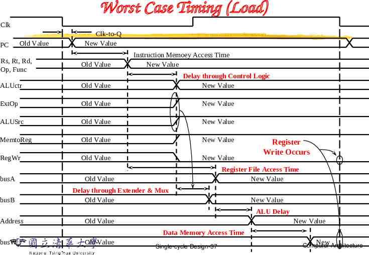
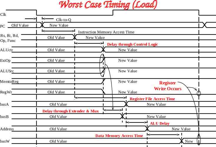
Worst Case Timing (Load) Clk PC Old Value Clk-to-Q New Value Instruction Memoey Access Time New Value Rs, Rt, Rd, Op, Func Old Value ALUctr Old Value ExtOp Old Value New Value ALUSrc Old Value New Value MemtoReg Old Value New Value RegWr Old Value New Value busA busB Delay through Control Logic New Value Register Write Occurs Register File Access Time New Value Old Value Delay through Extender & Mux Old Value New Value ALU Delay Address Old Value New Value Data Memory Access Time busW Old Value Single-cycle Design-37 New Computer Architecture
Outline Introduction to designing a processor Analyzing the instruction set Building the datapath A single-cycle implementation Control for the single-cycle CPU Control of CPU operations (step 4) ALU controller Main controller Single-cycle Design-38 Computer Architecture
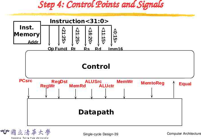
Step 4: Control Points and Signals Rd 0:15 Rs 11:15 Op Funct Rt 16:20 21:25 Addr 21:25 Inst. Memory Instruction 31:0 Imm16 Control PCsrc RegDst ALUSrc MemWr RegWr MemRd ALUctr MemtoReg Equal Datapath Single-cycle Design-39 Computer Architecture
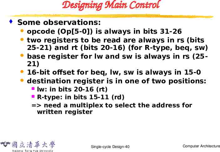
Designing Main Control Some observations: opcode (Op[5-0]) is always in bits 31-26 two registers to be read are always in rs (bits 25-21) and rt (bits 20-16) (for R-type, beq, sw) base register for lw and sw is always in rs (2521) 16-bit offset for beq, lw, sw is always in 15-0 destination register is in one of two positions: lw: in bits 20-16 (rt) R-type: in bits 15-11 (rd) need a multiplex to select the address for written register Single-cycle Design-40 Computer Architecture
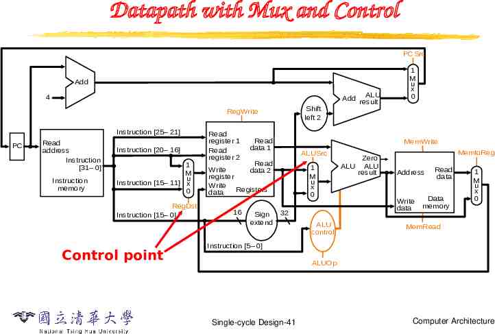
Datapath with Mux and Control PCSrc Add 4 Shift left 2 RegWrite Instruction [25– 21] PC Read address Instruction [31– 0] Instruction memory Instruction [20– 16] 1 M u Instruction [15– 11] x 0 RegDst Instruction [15– 0] Control point Read register 1 Read register 2 Read data 1 MemWrite ALUSrc Read Write data 2 register Write Registers data 16 Sign extend ALU Add result 1 M u x 0 1 M u x 0 32 ALU control Zero ALU ALU result MemtoReg Address Write data Read data Data memory 1 M u x 0 MemRead Instruction [5– 0] ALUOp Single-cycle Design-41 Computer Architecture
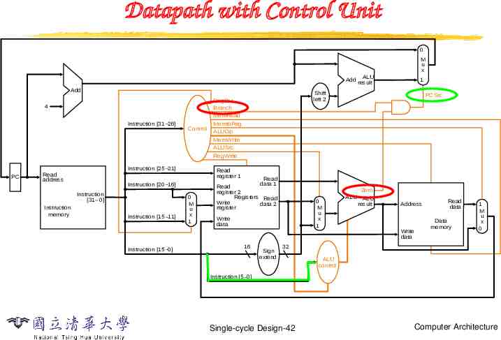
Datapath with Control Unit 0 M u x ALU Add result Add 4 Instruction [31 26] PC Instruction [25 21] Read address Instruction [15 11] Shift left 2 RegDst Branch MemRead MemtoReg ALUOp MemWrite ALUSrc RegWrite PCSrc Read register 1 Instruction [20 16] Instruction [31– 0] Instruction memory Control 1 0 M u x 1 Read data 1 Read register 2 Registers Read Write data 2 register 0 M u x 1 Write data Zero ALU ALU result Address Write data Instruction [15 0] 16 Sign extend Read data Data memory 1 M u x 0 32 ALU control Instruction [5 0] Single-cycle Design-42 Computer Architecture
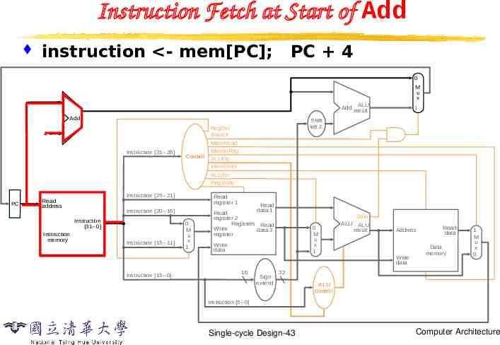
Instruction Fetch at Start of Add instruction - mem[PC]; PC 4 0 M u x Add Add 4 Instruction [31– 26] PC Instruction [25– 21] Read address Instruction [15– 11] 1 Shift left 2 RegDst Branch MemRead MemtoReg ALUOp MemWrite ALUSrc RegWrite Read register 1 Instruction [20– 16] Instruction [31– 0] Instruction memory Control ALU result 0 M u x 1 Read data 1 Read register 2 Registers Read Write data 2 register Zero 0 M u x 1 Write data ALU ALU result Address Write data Instruction [15– 0] 16 Sign extend Read data Data memory 1 M u x 0 32 ALU control Instruction [5– 0] Single-cycle Design-43 Computer Architecture
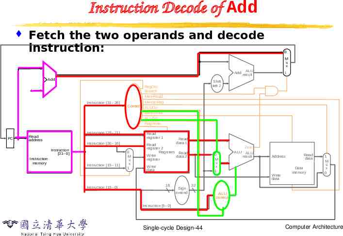
Instruction Decode of Add Fetch the two operands and decode instruction: 0 M u x Add Add 4 Instruction [31– 26] PC Instruction [25– 21] Read address Instruction [15– 11] 1 Shift left 2 RegDst Branch MemRead MemtoReg ALUOp MemWrite ALUSrc RegWrite Read register 1 Instruction [20– 16] Instruction [31– 0] Instruction memory Control ALU result 0 M u x 1 Read data 1 Read register 2 Registers Read Write data 2 register Zero 0 M u x 1 Write data ALU ALU result Address Write data Instruction [15– 0] 16 Sign extend Read data Data memory 1 M u x 0 32 ALU control Instruction [5– 0] Single-cycle Design-44 Computer Architecture
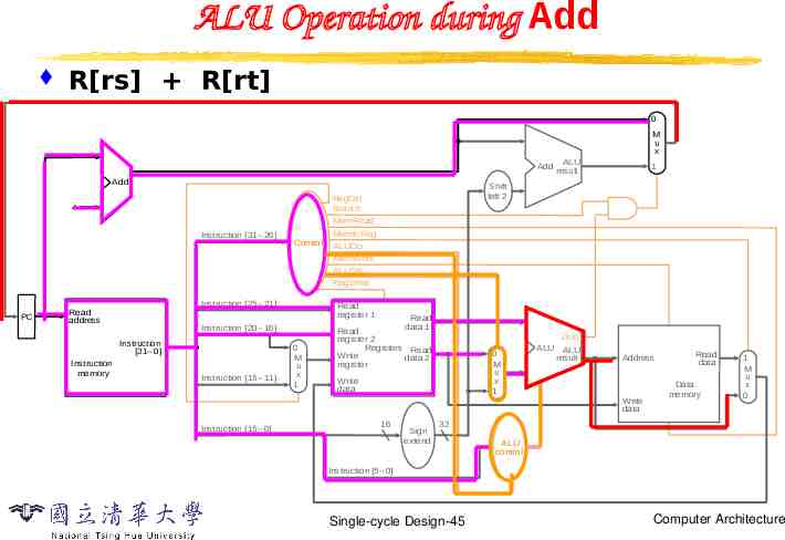
ALU Operation during Add R[rs] R[rt] 0 M u x Add Add 4 Instruction [31– 26] PC Instruction [25– 21] Read address Instruction [15– 11] 1 Shift left 2 RegDst Branch MemRead MemtoReg ALUOp MemWrite ALUSrc RegWrite Read register 1 Instruction [20– 16] Instruction [31– 0] Instruction memory Control ALU result 0 M u x 1 Read data 1 Read register 2 Registers Read Write data 2 register Zero 0 M u x 1 Write data ALU ALU result Address Write data Instruction [15– 0] 16 Sign extend Read data Data memory 1 M u x 0 32 ALU control Instruction [5– 0] Single-cycle Design-45 Computer Architecture
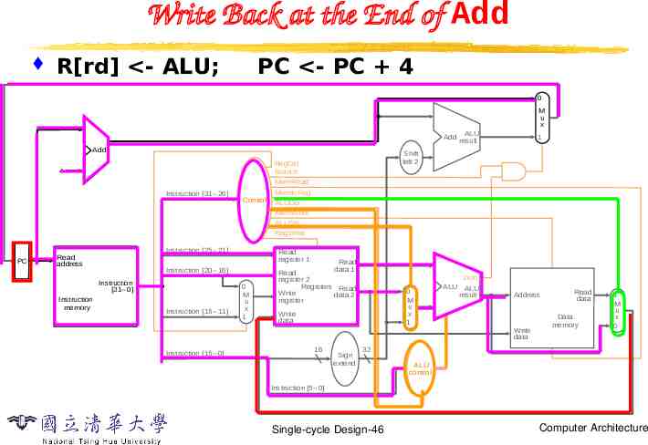
Write Back at the End of Add R[rd] - ALU; PC - PC 4 0 M u x Add Add 4 Instruction [31– 26] PC Instruction [25– 21] Read address Instruction [15– 11] 1 Shift left 2 RegDst Branch MemRead MemtoReg ALUOp MemWrite ALUSrc RegWrite Read register 1 Instruction [20– 16] Instruction [31– 0] Instruction memory Control ALU result 0 M u x 1 Read data 1 Read register 2 Registers Read Write data 2 register Zero 0 M u x 1 Write data ALU ALU result Address Write data Instruction [15– 0] 16 Sign extend Read data Data memory 1 M u x 0 32 ALU control Instruction [5– 0] Single-cycle Design-46 Computer Architecture
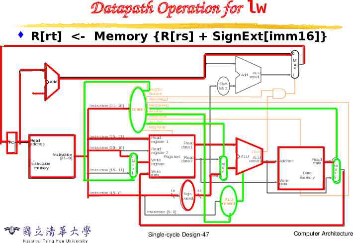
Datapath Operation for lw R[rt] - Memory {R[rs] SignExt[imm16]} 0 M u x Add Add 4 Instruction [31– 26] PC Instruction [25– 21] Read address Instruction [15– 11] 1 Shift left 2 RegDst Branch MemRead MemtoReg ALUOp MemWrite ALUSrc RegWrite Read register 1 Instruction [20– 16] Instruction [31– 0] Instruction memory Control ALU result 0 M u x 1 Read data 1 Read register 2 Registers Read Write data 2 register Zero 0 M u x 1 Write data ALU ALU result Address Write data Instruction [15– 0] 16 Sign extend Read data Data memory 1 M u x 0 32 ALU control Instruction [5– 0] Single-cycle Design-47 Computer Architecture
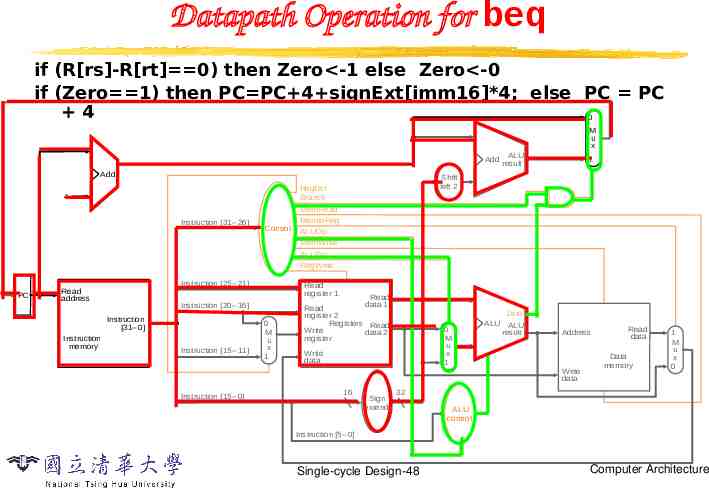
Datapath Operation for beq if (R[rs]-R[rt] 0) then Zero -1 else Zero -0 if (Zero 1) then PC PC 4 signExt[imm16]*4; else PC PC 4 0 M u x Add Add 4 Instruction [31– 26] PC Instruction [25– 21] Read address Instruction [15– 11] 1 Shift left 2 RegDst Branch MemRead MemtoReg ALUOp MemWrite ALUSrc RegWrite Read register 1 Instruction [20– 16] Instruction [31– 0] Instruction memory Control ALU result 0 M u x 1 Read data 1 Read register 2 Registers Read Write data 2 register Zero 0 M u x 1 Write data ALU ALU result Address Write data Instruction [15– 0] 16 Sign extend Read data Data memory 1 M u x 0 32 ALU control Instruction [5– 0] Single-cycle Design-48 Computer Architecture
Outline Designing a processor Analyzing the instruction set Building the datapath A single-cycle implementation Control for the single-cycle CPU Control of CPU operations ALU controller (step 5a) Main controller Single-cycle Design-49 Computer Architecture
Datapath with Control Unit 0 M u x ALU Add result Add 4 Instruction [31 26] PC Instruction [25 21] Read address Instruction [15 11] Shift left 2 RegDst Branch MemRead MemtoReg ALUOp MemWrite ALUSrc RegWrite PCSrc Read register 1 Instruction [20 16] Instruction [31– 0] Instruction memory Control 1 0 M u x 1 Read data 1 Read register 2 Registers Read Write data 2 register 0 M u x 1 Write data Zero ALU ALU result Address Write data Instruction [15 0] 16 Sign extend Read data Data memory 1 M u x 0 32 ALU control Instruction [5 0] Single-cycle Design-50 Computer Architecture
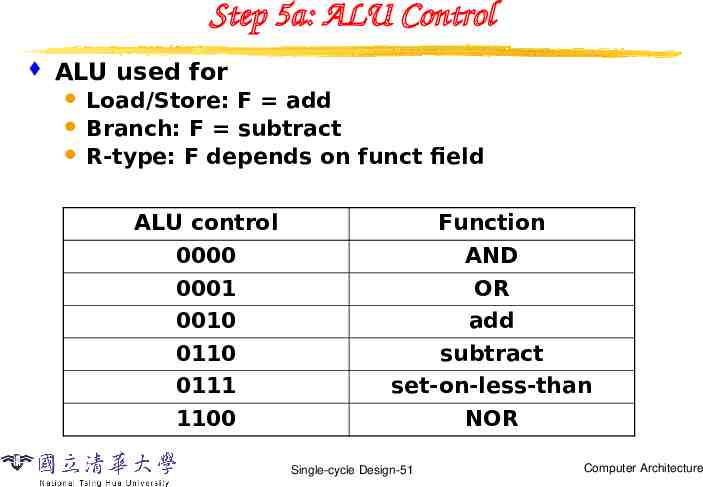
Step 5a: ALU Control ALU used for Load/Store: F add Branch: F subtract R-type: F depends on funct field ALU control 0000 0001 0010 0110 0111 1100 Function AND OR add subtract set-on-less-than NOR Single-cycle Design-51 Computer Architecture
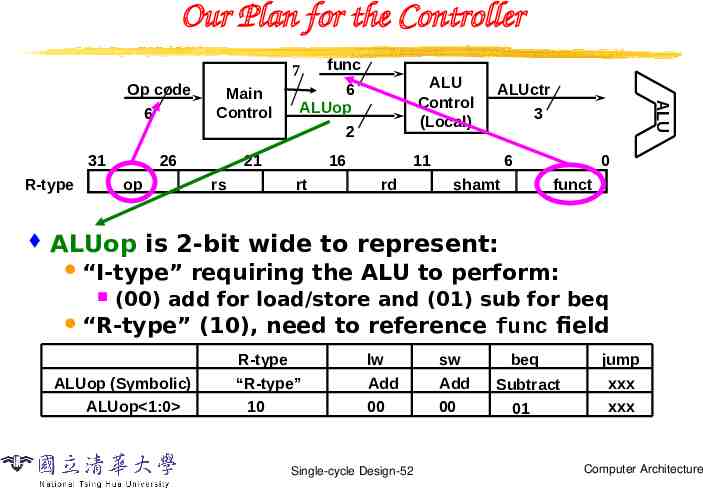
Our Plan for the Controller 7 Op code ALU Control (Local) 6 ALUop 2 31 R-type 26 21 op ALUop rs rt 3 11 rd 6 shamt 0 funct is 2-bit wide to represent: “I-type” 16 ALUctr ALU 6 Main Control func requiring the ALU to perform: (00) add for load/store and (01) sub for beq “R-type” ALUop (Symbolic) ALUop 1:0 (10), need to reference func field R-type lw sw “R-type” Add Add 00 00 10 Single-cycle Design-52 beq jump Subtract xxx 01 xxx Computer Architecture
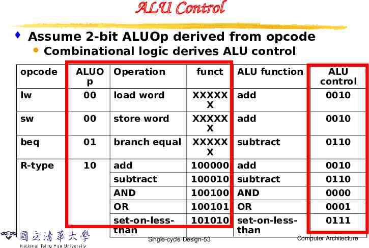
ALU Control Assume 2-bit ALUOp derived from opcode Combinational logic derives ALU control opcode Operation funct lw ALUO p 00 load word sw 00 store word beq 01 branch equal R-type 10 add subtract AND OR set-on-lessthan XXXXX X XXXXX X XXXXX X 100000 100010 100100 100101 101010 Single-cycle Design-53 ALU function add ALU control 0010 add 0010 subtract 0110 add subtract AND OR set-on-lessthan 0010 0110 0000 0001 0111 Computer Architecture
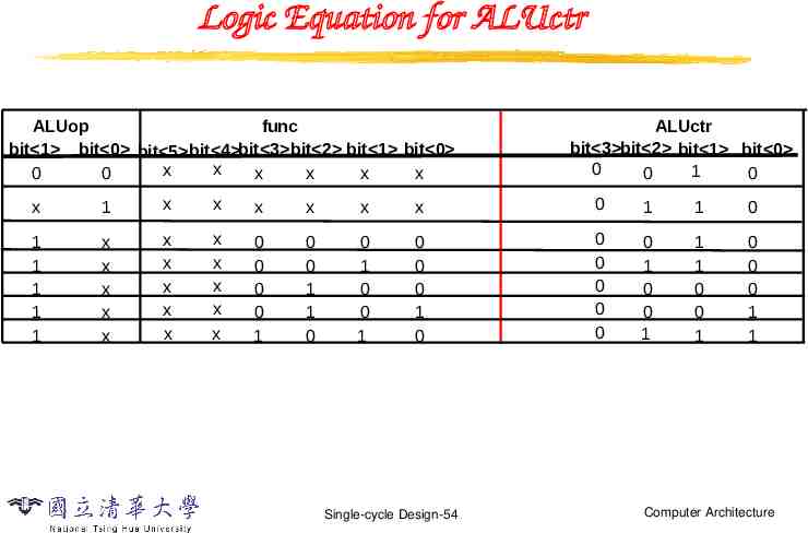
Logic Equation for ALUctr ALUop func bit 1 bit 0 bit 5 bit 4 bit 3 bit 2 bit 1 bit 0 x x 0 0 x x x x ALUctr bit 3 bit 2 bit 1 bit 0 0 1 0 0 x 1 x x x x x x 0 1 1 0 1 1 1 1 1 x x x x x x x x x x x x x x x 0 0 0 0 1 0 0 1 1 0 0 1 0 0 1 0 0 0 1 0 0 0 0 0 0 0 1 0 0 1 1 1 0 0 1 0 0 0 1 1 Single-cycle Design-54 Computer Architecture
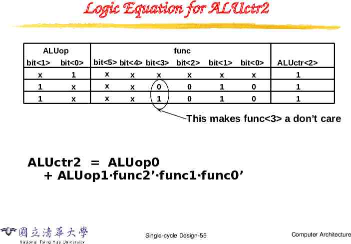
Logic Equation for ALUctr2 ALUop func bit 1 bit 0 x 1 1 x 1 x bit 5 bit 4 bit 3 bit 2 x x x x x x 0 0 x x 1 0 bit 1 bit 0 ALUctr 2 x x 1 1 0 1 1 0 1 This makes func 3 a don’t care ALUctr2 ALUop0 ALUop1‧func2’‧func1‧func0’ Single-cycle Design-55 Computer Architecture
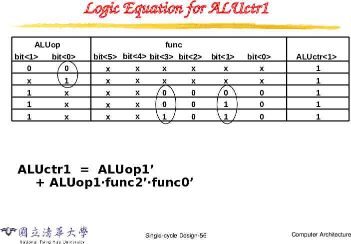
Logic Equation for ALUctr1 ALUop bit 1 func bit 0 bit 5 bit 4 bit 3 bit 2 x x x x x x x x x 0 0 x 0 0 x 1 1 x 1 x x x 0 1 x x x 1 bit 1 bit 0 ALUctr 1 x x 1 x x 1 0 0 1 0 1 0 1 0 1 0 1 ALUctr1 ALUop1’ ALUop1‧func2’‧func0’ Single-cycle Design-56 Computer Architecture
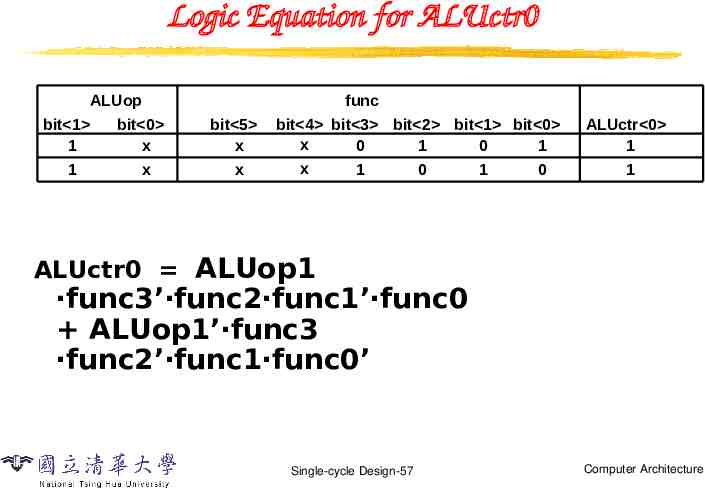
Logic Equation for ALUctr0 ALUop bit 1 1 1 bit 0 x x func bit 5 x x bit 4 bit 3 bit 2 bit 1 bit 0 x 0 1 0 1 x 1 0 1 0 ALUctr 0 1 1 ALUctr0 ALUop1 ‧func3’‧func2‧func1’‧func0 ALUop1’‧func3 ‧func2’‧func1‧func0’ Single-cycle Design-57 Computer Architecture
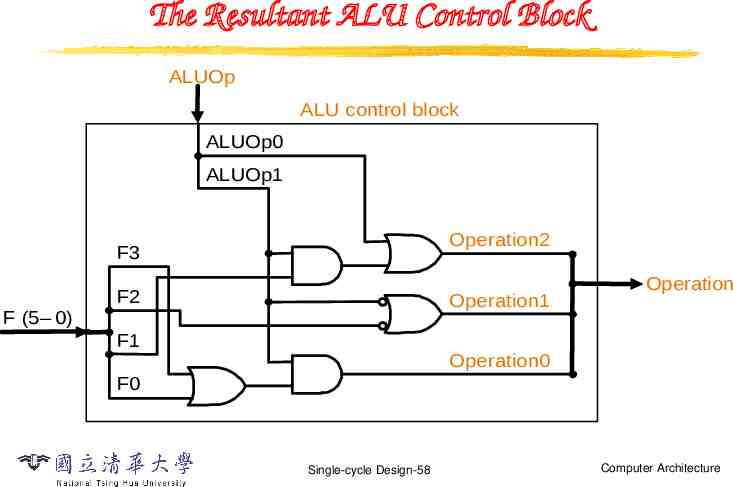
The Resultant ALU Control Block ALUOp ALU control block ALUOp0 ALUOp1 Operation2 F3 F (5– 0) F2 Operation1 F1 Operation Operation0 F0 Single-cycle Design-58 Computer Architecture
Outline Introduction to designing a processor Analyzing the instruction set Building the datapath A single-cycle implementation Control for the single-cycle CPU Control of CPU operations ALU controller Main controller (step 5b) Single-cycle Design-59 Computer Architecture
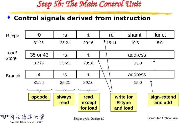
Step 5b: The Main Control Unit Control signals derived from instruction R-type Load/ Store Branch 0 rs rt rd shamt funct 31:26 25:21 20:16 15:11 10:6 5:0 35 or 43 rs rt address 31:26 25:21 20:16 15:0 4 rs rt address 31:26 25:21 20:16 15:0 opcode always read read, except for load Single-cycle Design-60 write for R-type and load sign-extend and add Computer Architecture
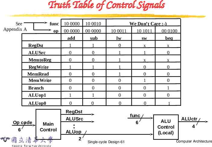
Truth Table of Control Signals See Appendix A func 10 0000 10 0010 op 00 0000 00 0000 10 0011 10 1011 00 0100 add sub lw sw beq RegDst 1 1 0 x x ALUSrc 0 0 1 1 0 MemtoReg 0 0 1 x x RegWrite MemRead MemWrite 1 0 0 1 0 0 1 1 0 0 0 1 0 0 0 Branch 0 0 0 0 1 ALUop1 1 1 0 0 0 ALUop0 0 0 0 0 1 Op code 6 Main Control We Don’t Care :-) RegDst ALUSrc func 6 : ALUop 2 Single-cycle Design-61 ALU Control (Local) ALUctr 4 Computer Architecture
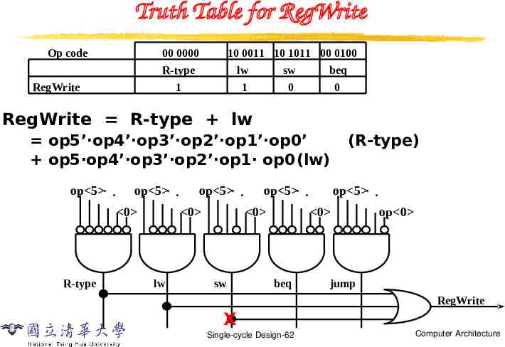
Truth Table for RegWrite Op code 00 0000 10 0011 10 1011 00 0100 R-type lw sw beq 1 1 0 0 RegWrite RegWrite R-type lw op5’‧op4’‧op3’‧op2’‧op1’‧op0’ op5‧op4’‧op3’‧op2’‧op1‧ op0(lw) op 5 . . op 5 . . 0 R-type op 5 . . 0 lw op 5 . . 0 sw (R-type) op 5 . . 0 beq op 0 jump RegWrite X Single-cycle Design-62 Computer Architecture
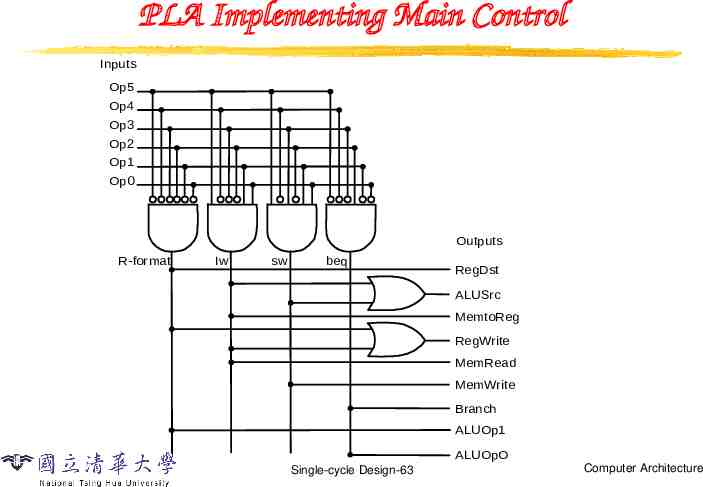
PLA Implementing Main Control Inputs Op5 Op4 Op3 Op2 Op1 Op0 Outputs R-format Iw sw beq RegDst ALUSrc MemtoReg RegWrite MemRead MemWrite Branch ALUOp1 ALUOpO Single-cycle Design-63 Computer Architecture
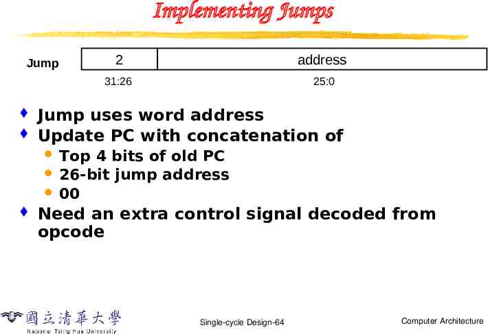
Implementing Jumps Jump 2 address 31:26 25:0 Jump uses word address Update PC with concatenation of Top 4 bits of old PC 26-bit jump address 00 Need an extra control signal decoded from opcode Single-cycle Design-64 Computer Architecture
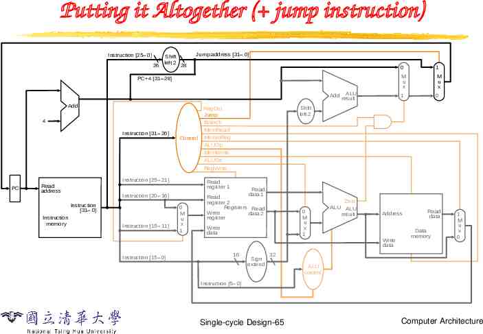
Putting it Altogether ( jump instruction) Instruction [25– 0] 26 Shift left 2 Jump address [31– 0] 28 0 1 M u x M u x ALU Add result 1 0 Zero ALU ALU result Address PC 4 [31– 28] Add 4 Instruction [31– 26] PC Instruction [25– 21] Read address Read register 1 Instruction [20– 16] Instruction [31– 0] Instruction memory Control Instruction [15– 11] Shift left 2 RegDst Jump Branch MemRead MemtoReg ALUOp MemWrite ALUSrc RegWrite 0 M u x 1 Read data 1 Read register 2 Registers Read Write data 2 register 0 M u x 1 Write data Write data Instruction [15– 0] 16 Sign extend Read data Data memory 1 M u x 0 32 ALU control Instruction [5– 0] Single-cycle Design-65 Computer Architecture
Worst Case Timing (Load) Clk PC Old Value Clk-to-Q New Value Instruction Memoey Access Time New Value Rs, Rt, Rd, Op, Func Old Value ALUctr Old Value ExtOp Old Value New Value ALUSrc Old Value New Value MemtoReg Old Value New Value RegWr Old Value New Value busA busB Delay through Control Logic New Value Register Write Occurs Register File Access Time New Value Old Value Delay through Extender & Mux Old Value New Value ALU Delay Address Old Value New Value Data Memory Access Time busW Old Value New
Drawback of Single-Cycle Design Long cycle time: Cycle time must be long enough for the load instruction: PC’s Clock -to-Q Instruction Memory Access Time Register File Access Time ALU Delay (address calculation) Data Memory Access Time Register File Setup Time Clock Skew Cycle time for load is much longer than needed for all other instructions Single-cycle Design-67 Computer Architecture
Summary Single cycle datapath CPI 1, Clock cycle time long MIPS makes control easier Instructions same size Source registers always in same place Immediates same size, location Operations always on registers/immediates Single-cycle Design-68 Computer Architecture