Chip Synthesis review


86 Slides743.00 KB
Chip Synthesis review
Design Flow Spec Select Architecture Code RTL RTL Code Check RTL Testbench Floorplan CWLM Synthesis RTL Verification Formal Verification Logic Synthesis Test (Scan/JTAG) Power Reduction Datapath Synthesis Constraint s Lib DW Gate-level netlist/db ATPG Gate-level Verification Static Timing Analysis GDSII Physical Design Placement Info
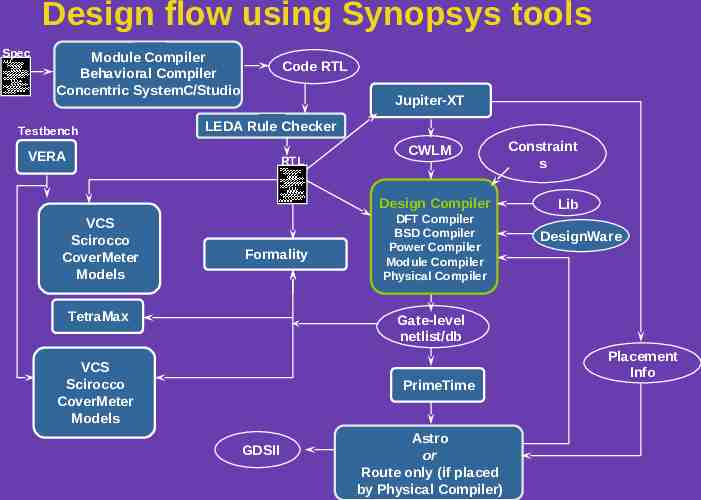
Design flow using Synopsys tools Spec Module Compiler Behavioral Compiler Concentric SystemC/Studio Testbench Code RTL Jupiter-XT LEDA Rule Checker VERA RTL CWLM Design Compiler VCS Scirocco CoverMeter Models Formality TetraMax DFT Compiler BSD Compiler Power Compiler Module Compiler Physical Compiler Constraint s Lib DesignWare Gate-level netlist/db VCS Scirocco CoverMeter Models PrimeTime GDSII Astro or Route only (if placed by Physical Compiler) Placement Info
What is Synthesis Synthesis is the transformation of an idea into a manufacturable device to carry out an intended function.
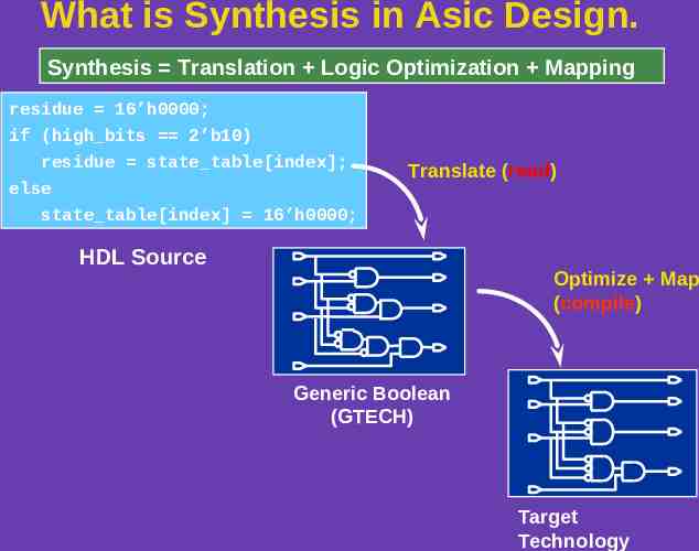
What is Synthesis in Asic Design. Synthesis Translation Logic Optimization Mapping residue 16’h0000; if (high bits 2’b10) residue state table[index]; else Translate (read) state table[index] 16’h0000; HDL Source Optimize Map (compile) Generic Boolean (GTECH) Target Technology
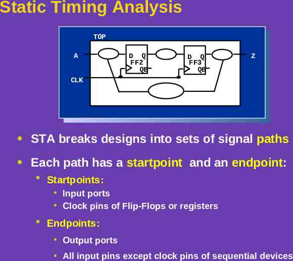
Static Timing Analysis TOP A D Q FF2 QB D Q FF3 QB Z CLK STA breaks designs into sets of signal paths Each path has a startpoint and an endpoint: Startpoints: Input ports Clock pins of Flip-Flops or registers Endpoints: Output ports All input pins except clock pins of sequential devices
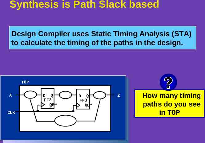
Synthesis is Path Slack based Design Compiler uses Static Timing Analysis (STA) to calculate the timing of the paths in the design. TOP A CLK D Q FF2 QB D Q FF3 QB Z How many timing paths do you see in TOP?
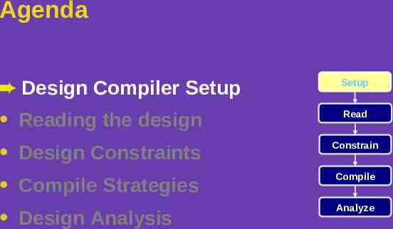
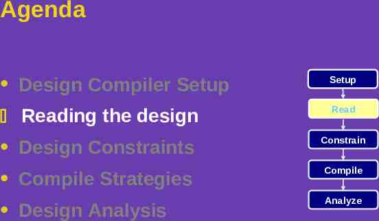
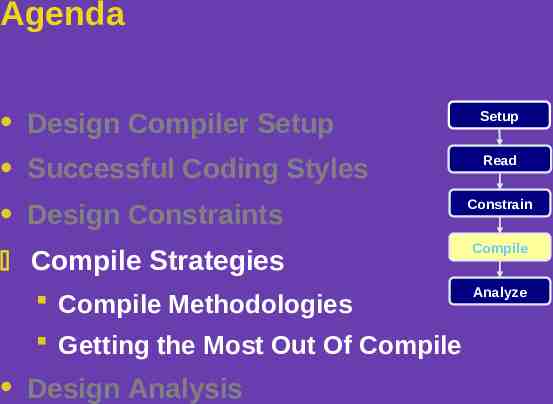
Agenda Design Compiler Setup Setup Reading the design Read Design Constraints Constrain Compile Strategies Compile Design Analysis Analyze
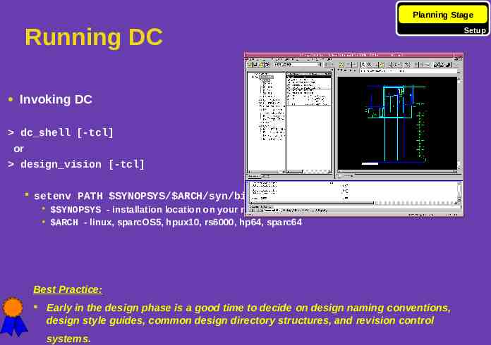
Planning Stage Running DC Invoking DC dc shell [-tcl] or design vision [-tcl] setenv PATH SYNOPSYS/ ARCH/syn/bin/dc shell SYNOPSYS - installation location on your network ARCH - linux, sparcOS5, hpux10, rs6000, hp64, sparc64 Best Practice: Early in the design phase is a good time to decide on design naming conventions, design style guides, common design directory structures, and revision control systems. Setup
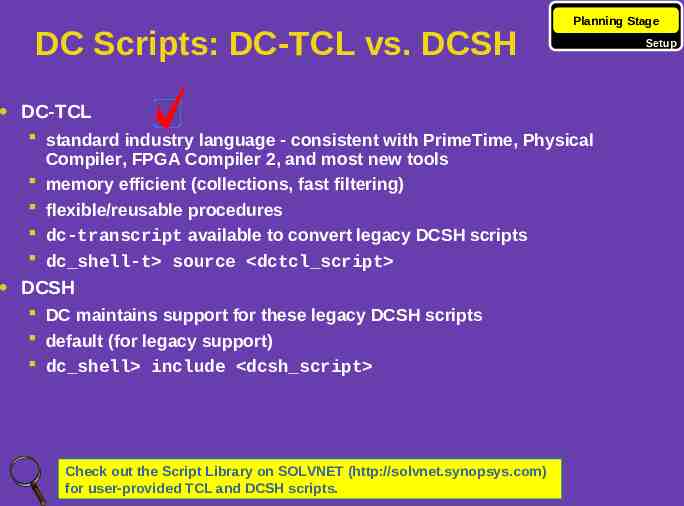
DC Scripts: DC-TCL vs. DCSH Planning Stage DC-TCL standard industry language - consistent with PrimeTime, Physical Compiler, FPGA Compiler 2, and most new tools memory efficient (collections, fast filtering) flexible/reusable procedures dc-transcript available to convert legacy DCSH scripts dc shell-t source dctcl script DCSH DC maintains support for these legacy DCSH scripts default (for legacy support) dc shell include dcsh script Check out the Script Library on SOLVNET (http://solvnet.synopsys.com) for user-provided TCL and DCSH scripts. Setup
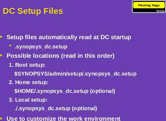
DC Setup Files Setup files automatically read at DC startup .synopsys dc.setup Possible locations (read in this order) 1. Root setup: SYNOPSYS/admin/setup/.synopsys dc.setup 2. Home setup: HOME/.synopsys dc.setup (optional) 3. Local setup: ./.synopsys dc.setup (optional) Use to customize the work environment Planning Stage Setup
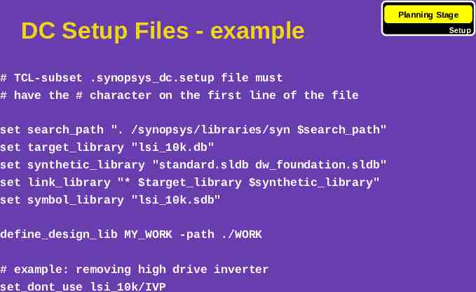
DC Setup Files - example # TCL-subset .synopsys dc.setup file must # have the # character on the first line of the file set search path ". /synopsys/libraries/syn search path" set target library "lsi 10k.db" set synthetic library "standard.sldb dw foundation.sldb" set link library "* target library synthetic library" set symbol library "lsi 10k.sdb" define design lib MY WORK -path ./WORK # example: removing high drive inverter set dont use lsi 10k/IVP Planning Stage Setup
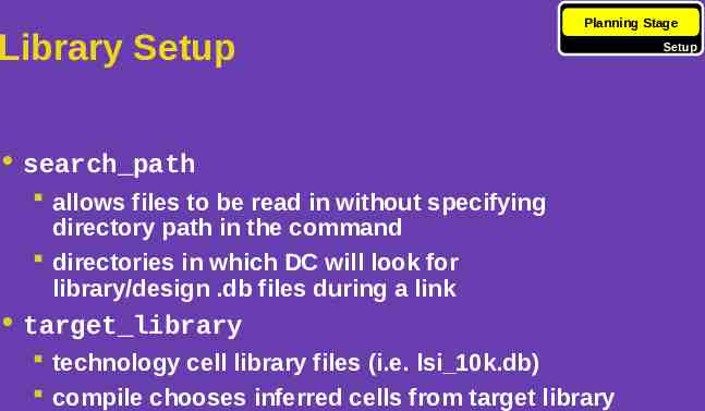
Library Setup Planning Stage search path allows files to be read in without specifying directory path in the command directories in which DC will look for library/design .db files during a link target library technology cell library files (i.e. lsi 10k.db) compile chooses inferred cells from target library Setup
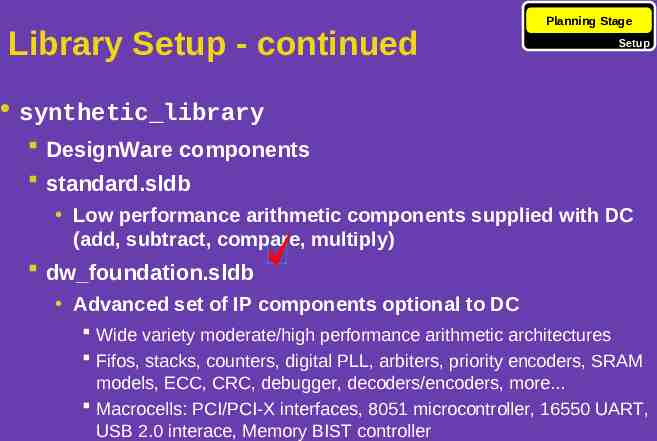
Library Setup - continued Planning Stage Setup synthetic library DesignWare components standard.sldb Low performance arithmetic components supplied with DC (add, subtract, compare, multiply) dw foundation.sldb Advanced set of IP components optional to DC Wide variety moderate/high performance arithmetic architectures Fifos, stacks, counters, digital PLL, arbiters, priority encoders, SRAM models, ECC, CRC, debugger, decoders/encoders, more. Macrocells: PCI/PCI-X interfaces, 8051 microcontroller, 16550 UART, USB 2.0 interace, Memory BIST controller
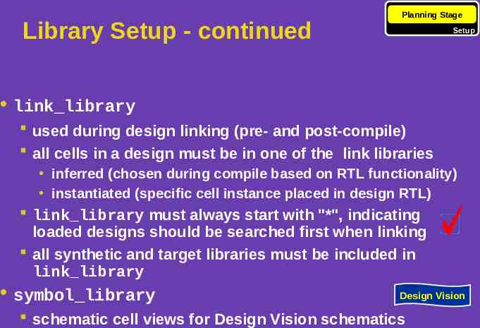
Library Setup - continued Planning Stage Setup link library used during design linking (pre- and post-compile) all cells in a design must be in one of the link libraries inferred (chosen during compile based on RTL functionality) instantiated (specific cell instance placed in design RTL) link library must always start with "*", indicating loaded designs should be searched first when linking all synthetic and target libraries must be included in link library symbol library Design Vision schematic cell views for Design Vision schematics
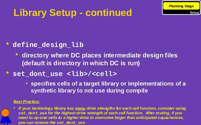
Library Setup - continued Planning Stage define design lib directory where DC places intermediate design files (default is directory in which DC is run) set dont use lib / cell specifies cells of a target library or implementations of a synthetic library to not use during compile Best Practice: If your technology library has many drive strengths for each cell function, consider using set dont use for the highest drive strength of each cell function. After routing, if you need to up-size cells to a higher drive to overcome larger than anticipated capacitances, you can remove the set dont use. Setup
Agenda Design Compiler Setup Reading the design Setup Read Design Constraints Constrain Compile Strategies Compile Design Analysis Analyze
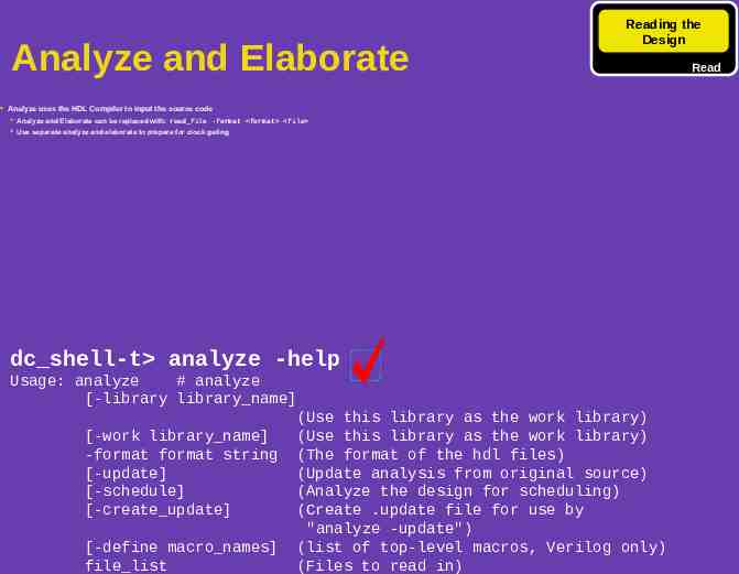
Analyze and Elaborate Reading the Design Analyze uses the HDL Compiler to input the source code Analyze and Elaborate can be replaced with: read file -format format file Use separate analyze and elaborate to prepare for clock gating dc shell-t analyze -help Usage: analyze # analyze [-library library name] (Use this library as the work library) [-work library name] (Use this library as the work library) -format format string (The format of the hdl files) [-update] (Update analysis from original source) [-schedule] (Analyze the design for scheduling) [-create update] (Create .update file for use by "analyze -update") [-define macro names] (list of top-level macros, Verilog only) file list (Files to read in) Read
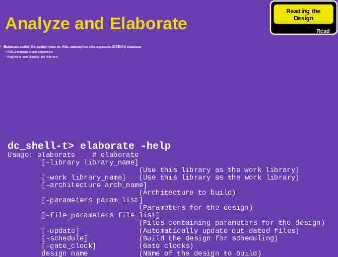
Analyze and Elaborate Reading the Design Read Elaborate builds the design from its HDL description into a generic (GTECH) database HDL parameters are expanded Registers and latches are inferred dc shell-t elaborate -help Usage: elaborate # elaborate [-library library name] (Use this library as the work library) [-work library name] (Use this library as the work library) [-architecture arch name] (Architecture to build) [-parameters param list] (Parameters for the design) [-file parameters file list] (Files containing parameters for the design) [-update] (Automatically update out-dated files) [-schedule] (Build the design for scheduling) [-gate clock] (Gate clocks) design name (Name of the design to build)
Agenda Design Compiler Setup Setup Successful Coding Styles Read Design Constraints Constrain Compile Strategies Compile Design Analysis Analyze
Design Constraints - Agenda Design Constraints Design Environment Defining Clocks Optimization Constraints Timing Exceptions
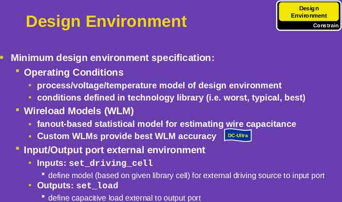
Design Environment Design Environment Constrain Minimum design environment specification: Operating Conditions process/voltage/temperature model of design environment conditions defined in technology library (i.e. worst, typical, best) Wireload Models (WLM) fanout-based statistical model for estimating wire capacitance Custom WLMs provide best WLM accuracy DC-Ultra Input/Output port external environment Inputs: set driving cell define model (based on given library cell) for external driving source to input port Outputs: set load define capacitive load external to output port
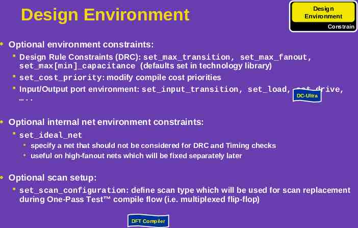
Design Environment Design Environment Constrain Optional environment constraints: Design Rule Constraints (DRC): set max transition, set max fanout, set max[min] capacitance (defaults set in technology library) set cost priority: modify compile cost priorities Input/Output port environment: set input transition, set load, set drive, DC-Ultra . Optional internal net environment constraints: set ideal net specify a net that should not be considered for DRC and Timing checks useful on high-fanout nets which will be fixed separately later Optional scan setup: set scan configuration: define scan type which will be used for scan replacement during One-Pass Test compile flow (i.e. multiplexed flip-flop) DFT Compiler
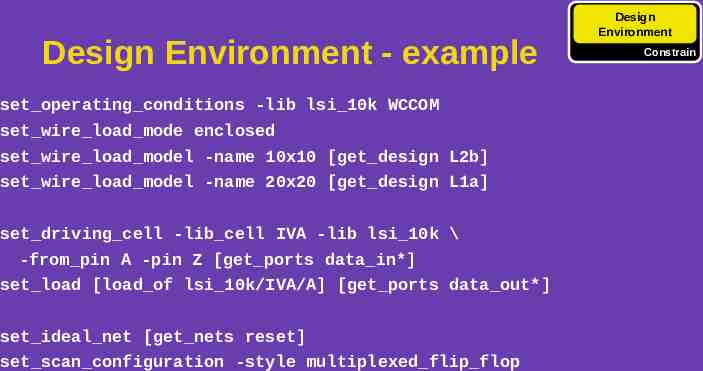
Design Environment - example set operating conditions -lib lsi 10k WCCOM set wire load mode enclosed set wire load model -name 10x10 [get design L2b] set wire load model -name 20x20 [get design L1a] set driving cell -lib cell IVA -lib lsi 10k \ -from pin A -pin Z [get ports data in*] set load [load of lsi 10k/IVA/A] [get ports data out*] set ideal net [get nets reset] set scan configuration -style multiplexed flip flop Design Environment Constrain
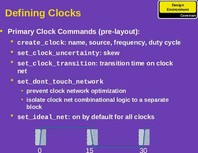
Design Environment Defining Clocks Constrain Primary Clock Commands (pre-layout): create clock: name, source, frequency, duty cycle set clock uncertainty: skew set clock transition: transition time on clock net set dont touch network prevent clock network optimization isolate clock net combinational logic to a separate block set ideal net: on by default for all clocks 0 15 30
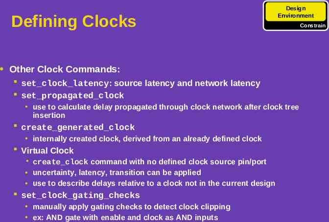
Defining Clocks Design Environment Other Clock Commands: set clock latency: source latency and network latency set propagated clock use to calculate delay propagated through clock network after clock tree insertion create generated clock internally created clock, derived from an already defined clock Virtual Clock create clock command with no defined clock source pin/port uncertainty, latency, transition can be applied use to describe delays relative to a clock not in the current design set clock gating checks manually apply gating checks to detect clock clipping ex: AND gate with enable and clock as AND inputs Constrain
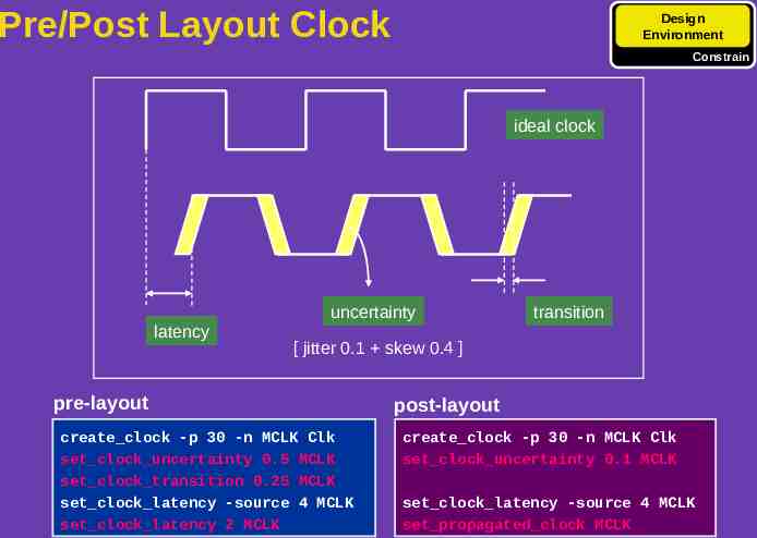
Pre/Post Layout Clock Design Environment Constrain ideal clock uncertainty latency transition [ jitter 0.1 skew 0.4 ] pre-layout create clock -p 30 -n MCLK Clk set clock uncertainty 0.5 MCLK set clock transition 0.25 MCLK set clock latency -source 4 MCLK set clock latency 2 MCLK post-layout create clock -p 30 -n MCLK Clk set clock uncertainty 0.1 MCLK set clock latency -source 4 MCLK set propagated clock MCLK
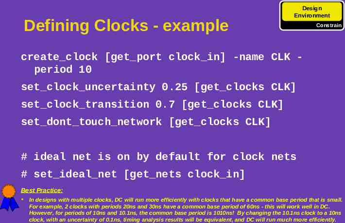
Defining Clocks - example Design Environment Constrain create clock [get port clock in] -name CLK period 10 set clock uncertainty 0.25 [get clocks CLK] set clock transition 0.7 [get clocks CLK] set dont touch network [get clocks CLK] # ideal net is on by default for clock nets # set ideal net [get nets clock in] Best Practice: In designs with multiple clocks, DC will run more efficiently with clocks that have a common base period that is small. For example, 2 clocks with periods 20ns and 30ns have a common base period of 60ns - this will work well in DC. However, for periods of 10ns and 10.1ns, the common base period is 1010ns! By changing the 10.1ns clock to a 10ns clock, with an uncertainty of 0.1ns, timing analysis results will be equivalent, and DC will run much more efficiently.
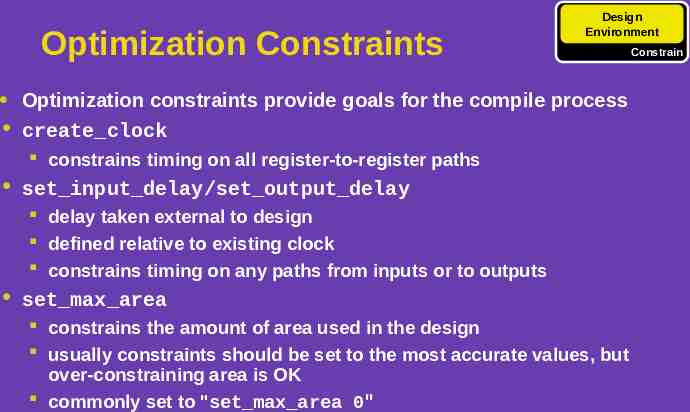
Optimization Constraints Design Environment Optimization constraints provide goals for the compile process create clock constrains timing on all register-to-register paths set input delay/set output delay delay taken external to design defined relative to existing clock constrains timing on any paths from inputs or to outputs set max area constrains the amount of area used in the design usually constraints should be set to the most accurate values, but over-constraining area is OK commonly set to "set max area 0" Constrain
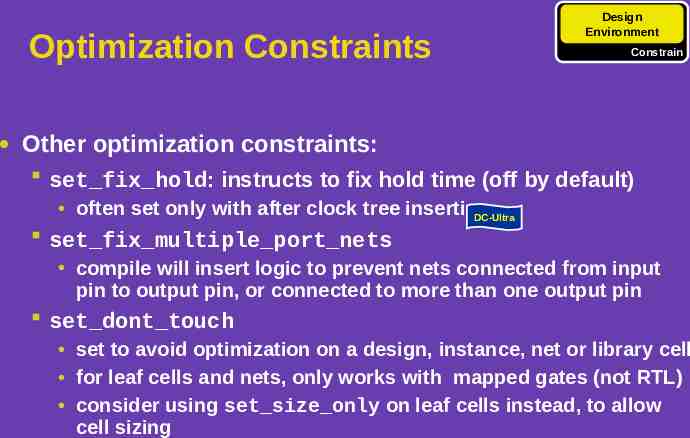
Optimization Constraints Design Environment Constrain Other optimization constraints: set fix hold: instructs to fix hold time (off by default) often set only with after clock tree insertion DC-Ultra set fix multiple port nets compile will insert logic to prevent nets connected from input pin to output pin, or connected to more than one output pin set dont touch set to avoid optimization on a design, instance, net or library cell for leaf cells and nets, only works with mapped gates (not RTL) consider using set size only on leaf cells instead, to allow cell sizing
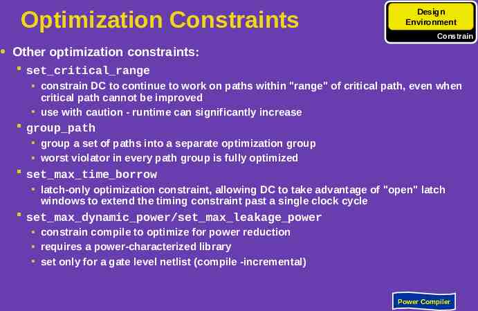
Optimization Constraints Design Environment Constrain Other optimization constraints: set critical range constrain DC to continue to work on paths within "range" of critical path, even when critical path cannot be improved use with caution - runtime can significantly increase group path group a set of paths into a separate optimization group worst violator in every path group is fully optimized set max time borrow latch-only optimization constraint, allowing DC to take advantage of "open" latch windows to extend the timing constraint past a single clock cycle set max dynamic power/set max leakage power constrain compile to optimize for power reduction requires a power-characterized library set only for a gate level netlist (compile -incremental) Power Compiler
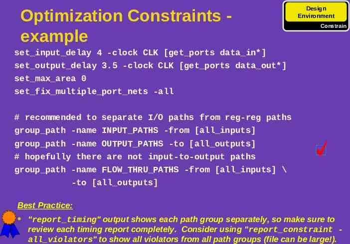
Optimization Constraints example Design Environment Constrain set input delay 4 -clock CLK [get ports data in*] set output delay 3.5 -clock CLK [get ports data out*] set max area 0 set fix multiple port nets -all # recommended to separate I/O paths from reg-reg paths group path -name INPUT PATHS -from [all inputs] group path -name OUTPUT PATHS -to [all outputs] # hopefully there are not input-to-output paths group path -name FLOW THRU PATHS -from [all inputs] \ -to [all outputs] Best Practice: "report timing" output shows each path group separately, so make sure to review each timing report completely. Consider using "report constraint all violators" to show all violators from all path groups (file can be large!).
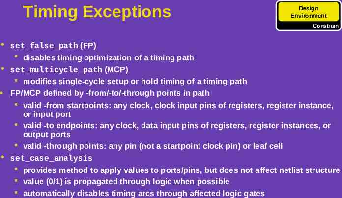
Timing Exceptions Design Environment Constrain set false path (FP) disables timing optimization of a timing path set multicycle path (MCP) modifies single-cycle setup or hold timing of a timing path FP/MCP defined by -from/-to/-through points in path valid -from startpoints: any clock, clock input pins of registers, register instance, or input port valid -to endpoints: any clock, data input pins of registers, register instances, or output ports valid -through points: any pin (not a startpoint clock pin) or leaf cell set case analysis provides method to apply values to ports/pins, but does not affect netlist structure value (0/1) is propagated through logic when possible automatically disables timing arcs through affected logic gates
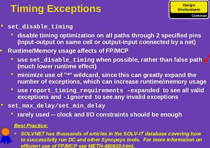
Timing Exceptions Design Environment Constrain set disable timing disable timing optimization on all paths through 2 specified pins (input-output on same cell or output-input connected by a net) Runtime/Memory usage affects of FP/MCP use set disable timing when possible, rather than false path (much lower runtime effect) minimize use of "*" wildcard, since this can greatly expand the number of exceptions, which can increase runtime/memory usage use report timing requirements -expanded to see all valid exceptions and -ignored to see any invalid exceptions set max delay/set min delay rarely used -- clock and I/O constraints should be enough Best Practice: SOLVNET has thousands of articles in the SOLV-IT database covering how to successfully run DC and other Synopsys tools. For more information on efficient use of FP/MCP see METH-480819.html.
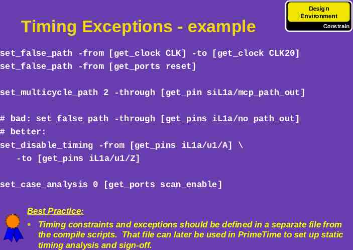
Timing Exceptions - example Design Environment Constrain set false path -from [get clock CLK] -to [get clock CLK20] set false path -from [get ports reset] set multicycle path 2 -through [get pin siL1a/mcp path out] # bad: set false path -through [get pins iL1a/no path out] # better: set disable timing -from [get pins iL1a/u1/A] \ -to [get pins iL1a/u1/Z] set case analysis 0 [get ports scan enable] Best Practice: Timing constraints and exceptions should be defined in a separate file from the compile scripts. That file can later be used in PrimeTime to set up static timing analysis and sign-off.
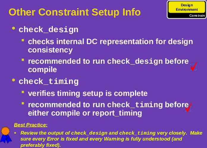
Other Constraint Setup Info Design Environment Constrain check design checks internal DC representation for design consistency recommended to run check design before compile check timing verifies timing setup is complete recommended to run check timing before either compile or report timing Best Practice: Review the output of check design and check timing very closely. Make sure every Error is fixed and every Warning is fully understood (and preferably fixed).
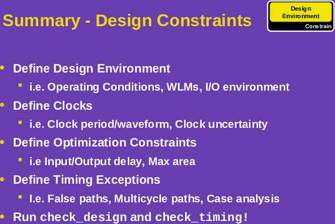
Summary - Design Constraints Design Environment Define Design Environment i.e. Operating Conditions, WLMs, I/O environment Define Clocks i.e. Clock period/waveform, Clock uncertainty Define Optimization Constraints i.e Input/Output delay, Max area Define Timing Exceptions I.e. False paths, Multicycle paths, Case analysis Run check design and check timing! Constrain
Agenda Design Compiler Setup Setup Successful Coding Styles Read Design Constraints Compile Strategies Compile Methodologies Getting the Most Out Of Compile Design Analysis Constrain Compile Analyze
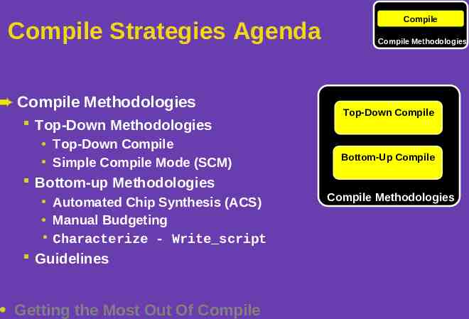
Compile Strategies Agenda Compile Methodologies Top-Down Methodologies Top-Down Compile Simple Compile Mode (SCM) Compile Compile Methodologies Top-Down Compile Bottom-Up Compile Bottom-up Methodologies Automated Chip Synthesis (ACS) Manual Budgeting Characterize - Write script Guidelines Getting the Most Out Of Compile Compile Methodologies
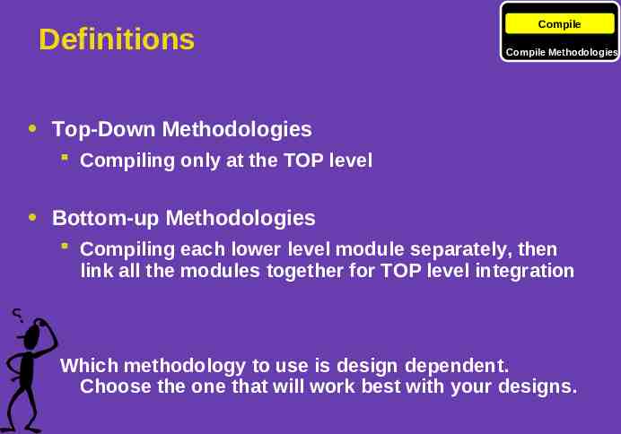
Definitions Compile Compile Methodologies Top-Down Methodologies Compiling only at the TOP level Bottom-up Methodologies Compiling each lower level module separately, then link all the modules together for TOP level integration Which methodology to use is design dependent. Choose the one that will work best with your designs.
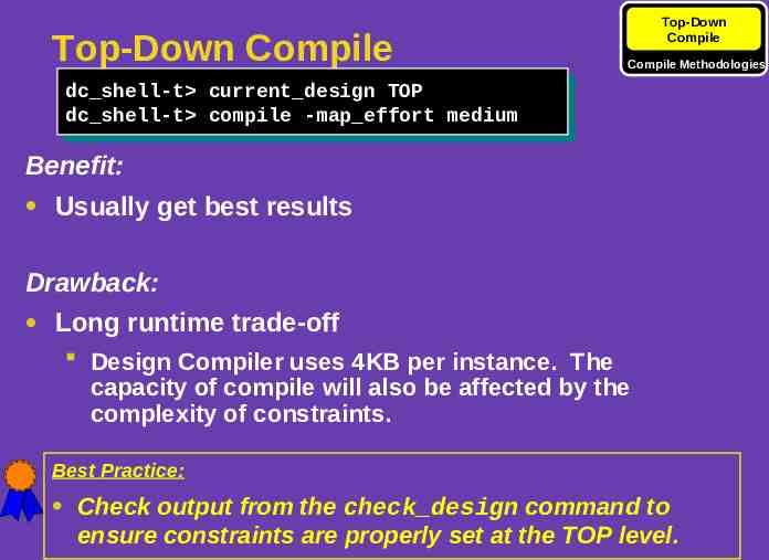
Top-Down Compile Top-Down Compile Compile Methodologies dc shell-t dc shell-t current design current design TOP TOP dc shell-t compile -map effort dc shell-t compile -map effort medium medium Benefit: Usually get best results Drawback: Long runtime trade-off Design Compiler uses 4KB per instance. The capacity of compile will also be affected by the complexity of constraints. Best Practice: Check output from the check design command to ensure constraints are properly set at the TOP level.
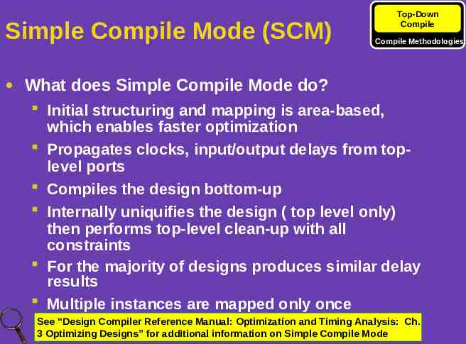
Simple Compile Mode (SCM) Top-Down Compile Compile Methodologies What does Simple Compile Mode do? Initial structuring and mapping is area-based, which enables faster optimization Propagates clocks, input/output delays from toplevel ports Compiles the design bottom-up Internally uniquifies the design ( top level only) then performs top-level clean-up with all constraints For the majority of designs produces similar delay results Multiple instances are mapped only once See “Design Compiler Reference Manual: Optimization and Timing Analysis: Ch. 3 Optimizing Designs” for additional information on Simple Compile Mode
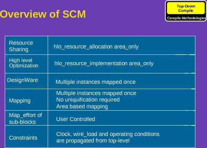
Overview of SCM Resource Sharing hlo resource allocation area only High level Optimization hlo resource implementation area only DesignWare Multiple instances mapped once Mapping Multiple instances mapped once No uniquification required Area based mapping Map effort of sub-blocks User Controlled Constraints Clock, wire load and operating conditions are propagated from top-level Top-Down Compile Compile Methodologies
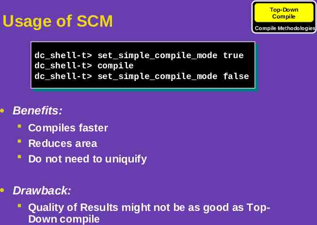
Usage of SCM Top-Down Compile Compile Methodologies dc shell-t dc shell-t set simple compile mode set simple compile mode true true dc shell-t dc shell-t compile compile dc shell-t dc shell-t set simple compile mode set simple compile mode false false Benefits: Compiles faster Reduces area Do not need to uniquify Drawback: Quality of Results might not be as good as TopDown compile
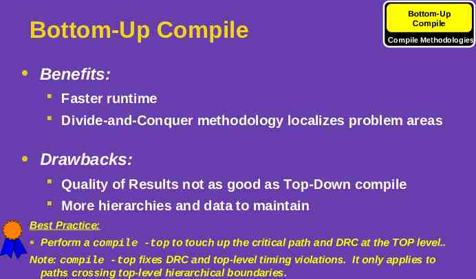
Bottom-Up Compile Bottom-Up Compile Compile Methodologies Benefits: Faster runtime Divide-and-Conquer methodology localizes problem areas Drawbacks: Quality of Results not as good as Top-Down compile More hierarchies and data to maintain Best Practice: Perform a compile -top to touch up the critical path and DRC at the TOP level. Note: compile -top fixes DRC and top-level timing violations. It only applies to paths crossing top-level hierarchical boundaries.
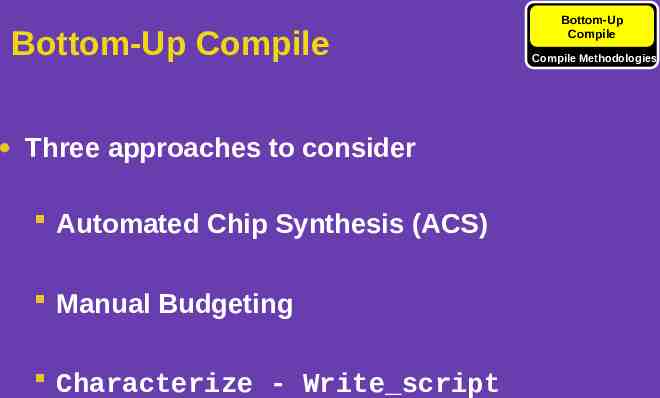
Bottom-Up Compile Three approaches to consider Automated Chip Synthesis (ACS) Manual Budgeting Characterize - Write script Bottom-Up Compile Compile Methodologies
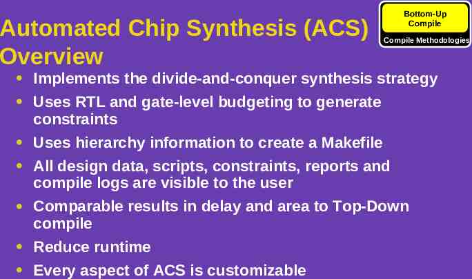
Automated Chip Synthesis (ACS) Overview Bottom-Up Compile Compile Methodologies Implements the divide-and-conquer synthesis strategy Uses RTL and gate-level budgeting to generate constraints Uses hierarchy information to create a Makefile All design data, scripts, constraints, reports and compile logs are visible to the user Comparable results in delay and area to Top-Down compile Reduce runtime Every aspect of ACS is customizable
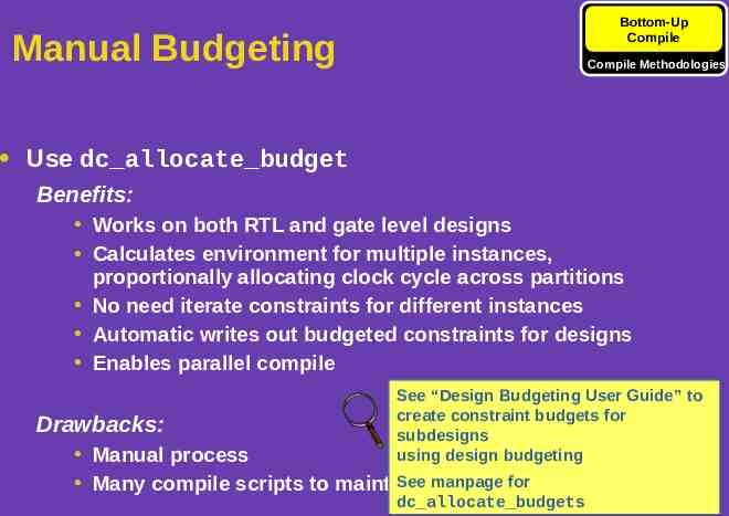
Bottom-Up Compile Manual Budgeting Compile Methodologies Use dc allocate budget Benefits: Works on both RTL and gate level designs Calculates environment for multiple instances, proportionally allocating clock cycle across partitions No need iterate constraints for different instances Automatic writes out budgeted constraints for designs Enables parallel compile Drawbacks: See “Design Budgeting User Guide” to create constraint budgets for subdesigns using design budgeting Manual process See manpage for Many compile scripts to maintain dc allocate budgets
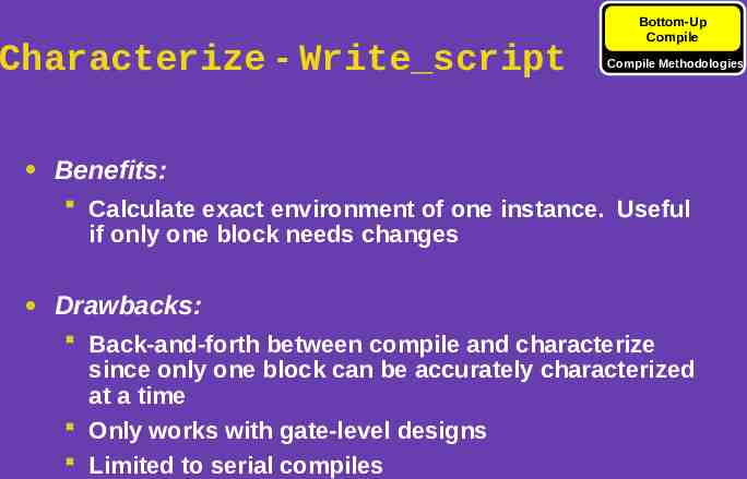
Characterize - Write script Bottom-Up Compile Compile Methodologies Benefits: Calculate exact environment of one instance. Useful if only one block needs changes Drawbacks: Back-and-forth between compile and characterize since only one block can be accurately characterized at a time Only works with gate-level designs Limited to serial compiles
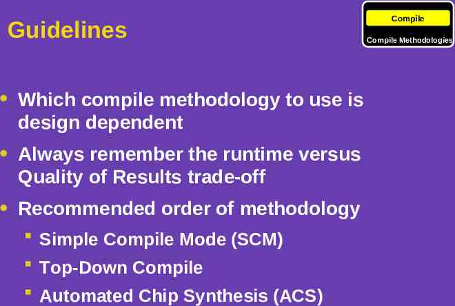
Guidelines Which compile methodology to use is design dependent Always remember the runtime versus Quality of Results trade-off Recommended order of methodology Simple Compile Mode (SCM) Top-Down Compile Automated Chip Synthesis (ACS) Compile Compile Methodologies
Take a Break!
Agenda Compile Compile Methodologies Getting the Most Out Of Compile Timing Area Timing Area Runtime/Capacity Runtime/Capacity Getting the Most Out Of Compile
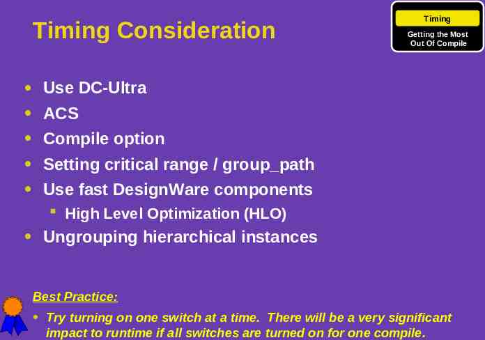
Timing Consideration Timing Getting the Most Out Of Compile Use DC-Ultra ACS Compile option Setting critical range / group path Use fast DesignWare components High Level Optimization (HLO) Ungrouping hierarchical instances Best Practice: Try turning on one switch at a time. There will be a very significant impact to runtime if all switches are turned on for one compile.
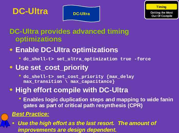
DC-Ultra Timing DC-Ultra Getting the Most Out Of Compile DC-Ultra provides advanced timing optimizations Enable DC-Ultra optimizations dc shell-t set ultra optimization true -force Use set cost priority dc shell-t set cost priority {max delay max transition \ max capacitance} High effort compile with DC-Ultra Enables logic duplication steps and mapping to wide fanin gates as part of critical path resynthesis (CPR) Best Practice: Use the high effort as the last resort. The amount of improvements are design dependent.
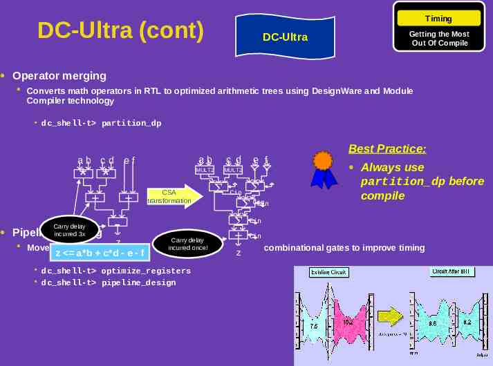
Timing DC-Ultra (cont) DC-Ultra Getting the Most Out Of Compile Operator merging Converts math operators in RTL to optimized arithmetic trees using DesignWare and Module Compiler technology dc shell-t partition dp ab c d ef * * Carry delay 3x retiming Pipelineincurred ab c d MULT2 MULT2 CSA transformation - z Moves registers through z a*b c*d - e - f Carry delay incurred once! dc shell-t optimize registers dc shell-t pipeline design Cin e f Cin Cin Cin Cin z Best Practice: Always use partition dp before compile combinational gates to improve timing
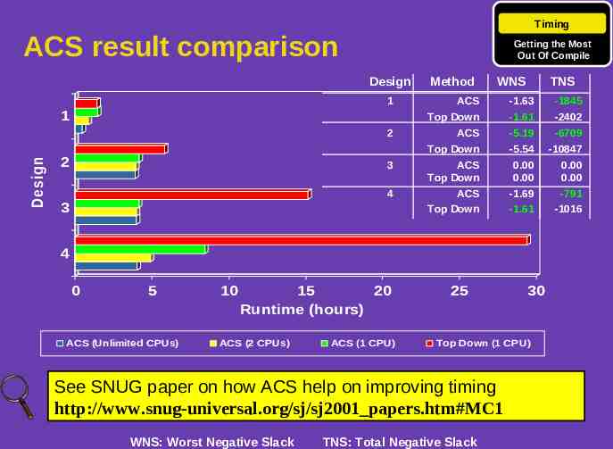
Timing ACS result comparison Getting the Most Out Of Compile Design 1 Design WNS TNS ACS -1.63 -1845 Top Down -1.61 -2402 2 ACS Top Down -5.19 -5.54 -6709 -10847 3 ACS Top Down ACS Top Down 0.00 0.00 -1.69 -1.61 0.00 0.00 -791 -1016 1 2 Method 4 3 4 0 5 ACS (Unlimited CPUs) 10 15 20 Runtime (hours) ACS (2 CPUs) ACS (1 CPU) 25 Top Down (1 CPU) See SNUG paper on how ACS help on improving timing http://www.snug-universal.org/sj/sj2001 papers.htm#MC1 WNS: Worst Negative Slack 30 TNS: Total Negative Slack
Compile Option Timing Getting the Most Out Of Compile Use high effort compile Best Practice: Use the high effort compile if you are within of 10% of meeting timing. The high effort compile switch will increase compile time significantly.
Setting Critical Range / Group Path Timing Getting the Most Out Of Compile Set a critical range Critical range specifies a margin of delay for path groups during optimization dc shell-t set critical range 2 TOP Group different path groups together and set a critical range dc shell-t group path -from [all inputs] -name \ input paths -critical range 0 dc shell-t group path -to [all outputs] -name \ output paths -critical range 0 dc shell-t group path -from clk -to clk -name \ internal paths -critical range 2 Best Practice: Use a reasonable amount for critical range (i.e. 10% of the clock period). The larger the critical range, the longer the compile time.
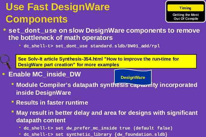
Use Fast DesignWare Components Timing Getting the Most Out Of Compile set dont use on slow DesignWare components to remove the bottleneck of math operators dc shell-t set dont use standard.sldb/DW01 add/rpl See Solv-It article Synthesis-354.html ”How to improve the run-time for DesigWare part creation” for more examples Enable MC inside DW DesignWare Module Compiler’s datapath synthesis capability incorporated inside DesignWare Results in faster runtime May result in better delay and area for designs with significant datapath content dc shell-t set dw prefer mc inside true (default false) dc shell-t set synthetic library {dw foundation.sldb}
Ungrouping Hierarchical Instances Timing Getting the Most Out Of Compile Ungroup along the critical path enables more mapping permutations Enable boundary optimization optimizations are limited within hierarchical boundaries, so enabling boundary optimization can further improve the critical path dc shell-t compile -boundary optimization
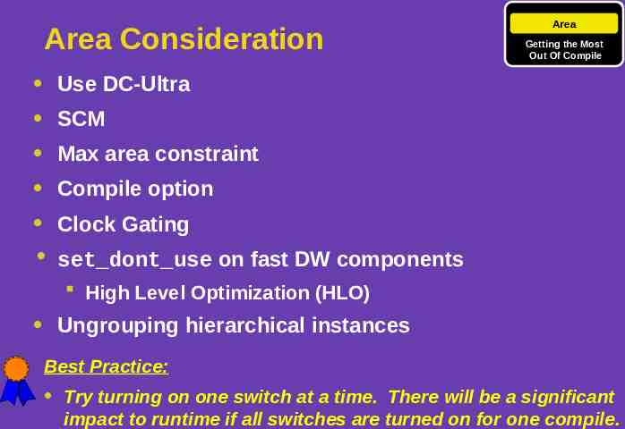
Area Consideration Compile Area Getting the Most Out Of Compile Use DC-Ultra SCM Max area constraint Compile option Clock Gating set dont use on fast DW components High Level Optimization (HLO) Ungrouping hierarchical instances Best Practice: Try turning on one switch at a time. There will be a significant impact to runtime if all switches are turned on for one compile.
DC-Ultra Compile Area DC-Ultra Getting the Most Out Of Compile Same set of rules also apply to area centric optimization High effort compile with DC-Ultra Enables logic duplication steps and mapping to wide fanin gates as part of critical path resynthesis (CPR) Operator merging dc shell-t partition dp Pipeline retiming dc shell-t optimize registers dc shell-t pipeline design
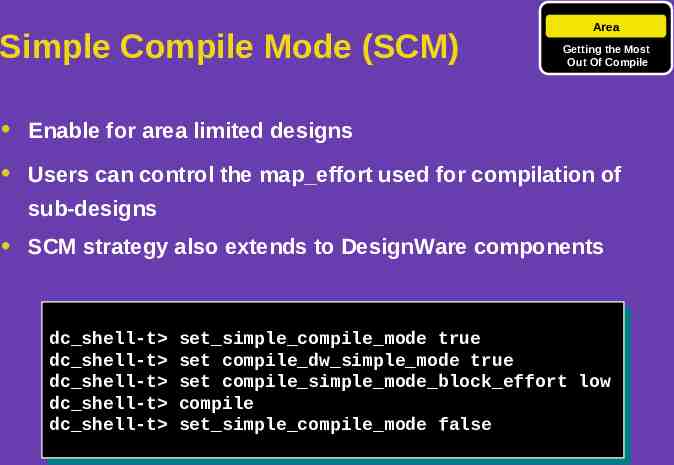
Compile Simple Compile Mode (SCM) Area Getting the Most Out Of Compile Enable for area limited designs Users can control the map effort used for compilation of sub-designs SCM strategy also extends to DesignWare components dc shell-t dc shell-t set simple compile mode set simple compile mode true true dc shell-t set compile dw simple mode dc shell-t set compile dw simple mode true true dc shell-t dc shell-t set set compile simple mode block effort compile simple mode block effort low low dc shell-t dc shell-t compile compile dc shell-t dc shell-t set simple compile mode set simple compile mode false false
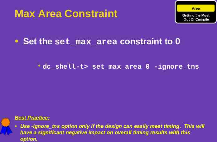
Max Area Constraint Compile Area Getting the Most Out Of Compile Set the set max area constraint to 0 dc shell-t set max area 0 -ignore tns Best Practice: Use -ignore tns option only if the design can easily meet timing. This will have a significant negative impact on overall timing results with this option.
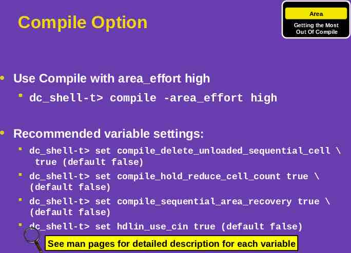
Compile Option Compile Area Getting the Most Out Of Compile Use Compile with area effort high dc shell-t compile -area effort high Recommended variable settings: dc shell-t set compile delete unloaded sequential cell \ true (default false) dc shell-t set compile hold reduce cell count true \ (default false) dc shell-t set compile sequential area recovery true \ (default false) dc shell-t set hdlin use cin true (default false) See man pages for detailed description for each variable
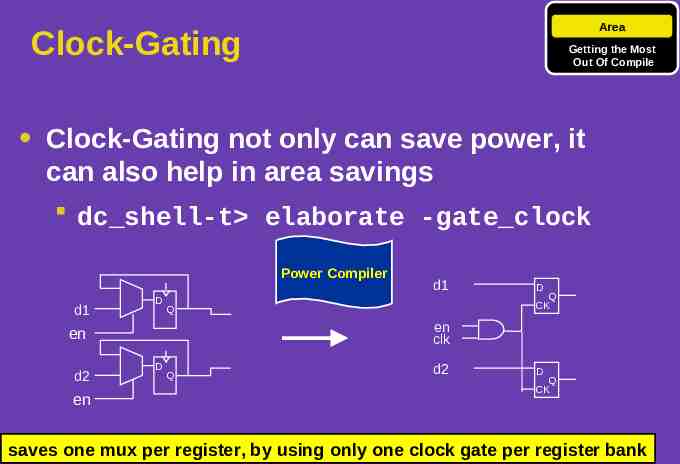
Compile Area Clock-Gating Getting the Most Out Of Compile Clock-Gating not only can save power, it can also help in area savings dc shell-t elaborate -gate clock Power Compiler d1 D Q en D Q CK en clk en d2 d1 D Q d2 D Q CK saves one mux per register, by using only one clock gate per register bank
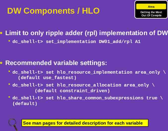
DW Components / HLO Compile Area Getting the Most Out Of Compile Limit to only ripple adder (rpl) implementation of DW dc shell-t set implementation DW01 add/rpl A1 Recommended variable settings: dc shell-t set hlo resource implementation area only \ (default use fastest) dc shell-t set hlo resource allocation area only \ (default constraint driven) dc shell-t set hlo share common subexpressions true \ (default) See man pages for detailed description for each variable
Compile Ungrouping Hierarchical Instances Ungrouping can also help save area Eliminate hierarchical boundaries dc shell-t ungroup -all -flatten Enable boundary optimization dc shell-t compile boundary optimization Area Getting the Most Out Of Compile
Runtime Methodology Runtime/Capacity Getting the Most Out Of Compile Use ACS or SCM Use low / medium effort compile set dont use certain implementations of DW minimize the choices during compile Watch for asynchronous clock domains should have a low common base period Specify timing exceptions efficiently with wildcard See Solv-It article Methodology-81.html “Specifying Effort Timing Exceptions Application Note” for more information
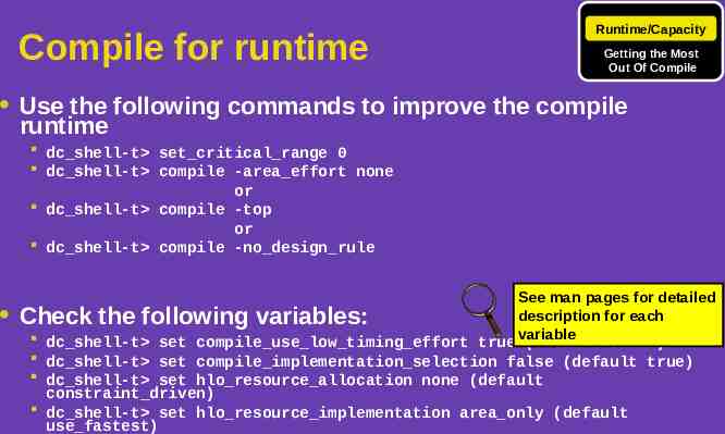
Compile for runtime Runtime/Capacity Getting the Most Out Of Compile Use the following commands to improve the compile runtime dc shell-t set critical range 0 dc shell-t compile -area effort none or dc shell-t compile -top or dc shell-t compile -no design rule See man pages for detailed description for each Check the following variables: dc shell-t set compile use low timing effort true variable (default false) dc shell-t set compile implementation selection false (default true) dc shell-t set hlo resource allocation none (default constraint driven) dc shell-t set hlo resource implementation area only (default use fastest)
Capacity Methodology Runtime/Capacity Getting the Most Out Of Compile What if I can’t read the top level into DC? Specify only the libraries needed in link library and target library Use netlist reader for Verilog gate level netlists dc shell-t read file -format verilog -netlist TOP.v Change system limit to 4GB See Solv-It article Synthesis-745.html “Memory Usage in Design Compiler” for information on how to set system limit to 4GB What if I can read the top level into DC? Use ACS Remove unused designs from memory
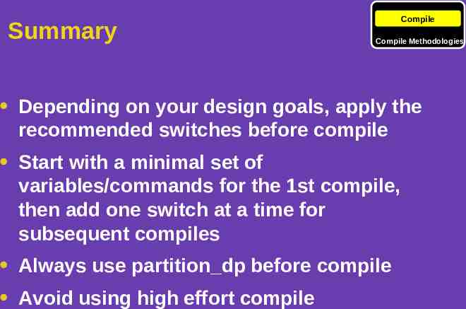
Summary Compile Compile Methodologies Depending on your design goals, apply the recommended switches before compile Start with a minimal set of variables/commands for the 1st compile, then add one switch at a time for subsequent compiles Always use partition dp before compile Avoid using high effort compile
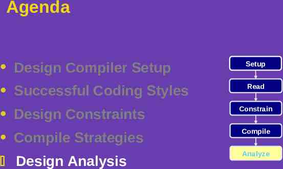
Agenda Design Compiler Setup Setup Successful Coding Styles Read Design Constraints Constrain Compile Strategies Compile Design Analysis Analyze
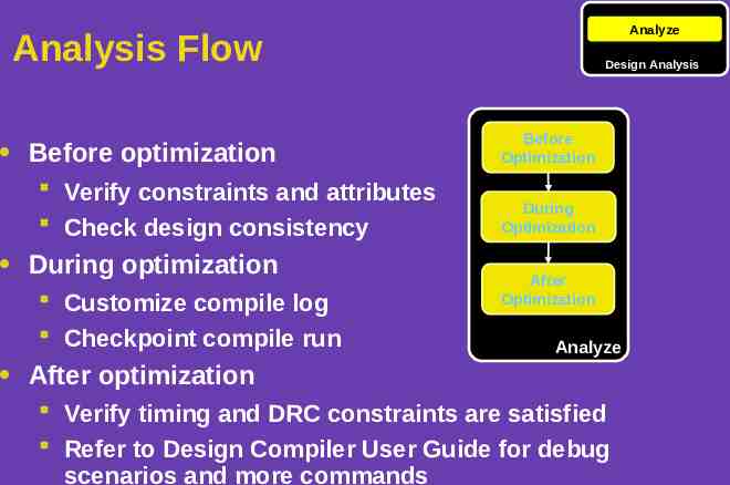
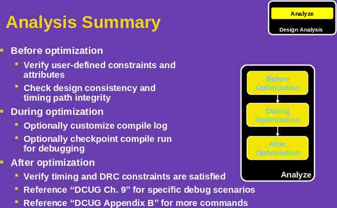
Analyze Analysis Flow Before optimization Verify constraints and attributes Check design consistency During optimization Customize compile log Checkpoint compile run After optimization Design Analysis Before Optimization During Optimization After Optimization Analyze Verify timing and DRC constraints are satisfied Refer to Design Compiler User Guide for debug scenarios and more commands
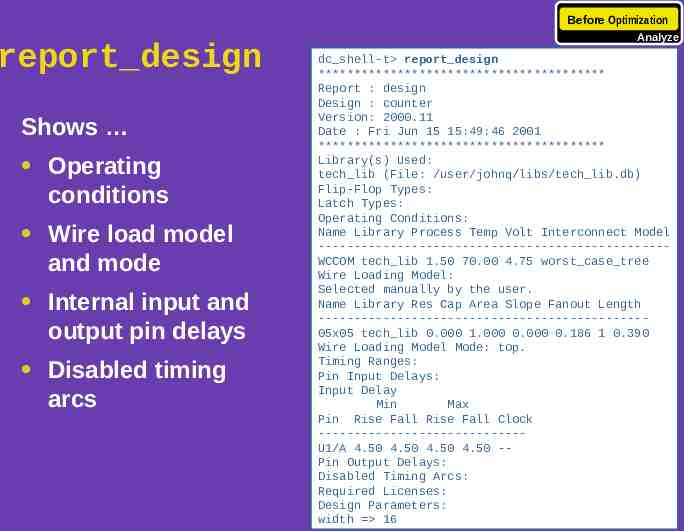
Before Optimization report design Shows Operating conditions Wire load model and mode Internal input and output pin delays Disabled timing arcs Analyze dc shell-t report design **************************************** Report : design Design : counter Version: 2000.11 Date : Fri Jun 15 15:49:46 2001 **************************************** Library(s) Used: tech lib (File: /user/johnq/libs/tech lib.db) Flip-Flop Types: Latch Types: Operating Conditions: Name Library Process Temp Volt Interconnect Model ------------------------------------------------WCCOM tech lib 1.50 70.00 4.75 worst case tree Wire Loading Model: Selected manually by the user. Name Library Res Cap Area Slope Fanout Length ---------------------------------------------05x05 tech lib 0.000 1.000 0.000 0.186 1 0.390 Wire Loading Model Mode: top. Timing Ranges: Pin Input Delays: Input Delay Min Max Pin Rise Fall Rise Fall Clock ----------------------------U1/A 4.50 4.50 4.50 4.50 -Pin Output Delays: Disabled Timing Arcs: Required Licenses: Design Parameters: width 16
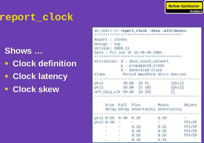
Before Optimization report clock Shows Clock definition Clock latency Clock skew Analyze dc shell-t report clock -skew -attributes **************************************** Report : clocks Design : top Version: 2000.11 Date : Fri Jun 15 15:49:46 2001 **************************************** Attributes: d - dont touch network p - propagated clock G - Generated clock Clock Period Waveform Attrs Sources -----------------------------------------------phi1 10.00 {0 5} {phi1} phi2 10.00 {5 10} {phi2} off chip clk 50.00 {0 25} {} -----------------------------------------------Rise Fall Plus Minus Object Delay Delay Uncertainty Uncertainty -----------------------------------------------phi1 0.50 0.40 0.20 0.10 phi2 0.20 ff1/CP 0.10 0.15 ff2/CP 0.10 0.15 ff3/CP 0.10 0.15 ff4/CP 0.10 0.15
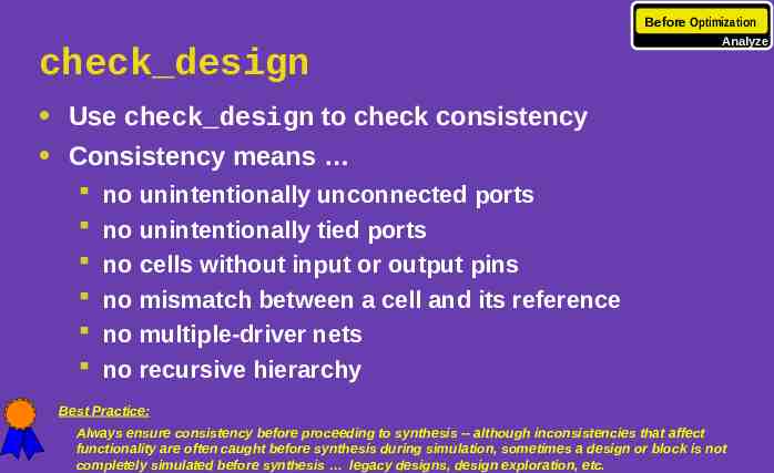
Before Optimization check design Analyze Use check design to check consistency Consistency means no unintentionally unconnected ports no unintentionally tied ports no cells without input or output pins no mismatch between a cell and its reference no multiple-driver nets no recursive hierarchy Best Practice: Always ensure consistency before proceeding to synthesis -- although inconsistencies that affect functionality are often caught before synthesis during simulation, sometimes a design or block is not completely simulated before synthesis legacy designs, design exploration, etc.
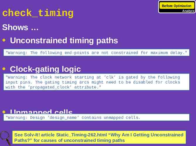
Before Optimization check timing Analyze Shows Unconstrained timing paths "Warning: The following end-points are not constrained for maximum delay." Clock-gating logic "Warning: The clock network starting at ’clk’ is gated by the following input pins. The gating timing arcs might need to be disabled for clocks with the ’propagated clock’ attribute." Unmapped cells "Warning: Design ’design name’ contains unmapped cells. See Solv-It! article Static Timing-262.html “Why Am I Getting Unconstrained Paths?” for causes of unconstrained timing paths
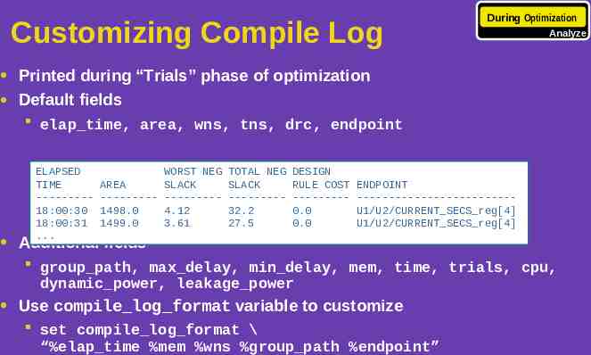
Customizing Compile Log During Optimization Analyze Printed during “Trials” phase of optimization Default fields elap time, area, wns, tns, drc, endpoint ELAPSED TIME --------18:00:30 18:00:31 . WORST NEG AREA SLACK --------- --------1498.0 4.12 1499.0 3.61 TOTAL NEG SLACK --------32.2 27.5 DESIGN RULE COST --------0.0 0.0 ENDPOINT ------------------------U1/U2/CURRENT SECS reg[4] U1/U2/CURRENT SECS reg[4] Additional fields group path, max delay, min delay, mem, time, trials, cpu, dynamic power, leakage power Use compile log format variable to customize set compile log format \ “%elap time %mem %wns %group path %endpoint”
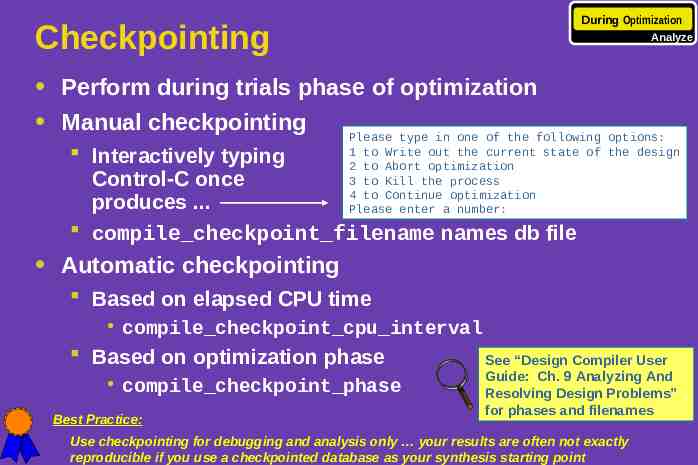
During Optimization Checkpointing Analyze Perform during trials phase of optimization Manual checkpointing Please type in one of the following options: 1 to Write out the current state Interactively typing 2 to Abort optimization 3 to Kill the process Control-C once 4 to Continue optimization produces . Please enter a number: compile checkpoint filename names db file of the design Automatic checkpointing Based on elapsed CPU time compile checkpoint cpu interval Based on optimization phase compile checkpoint phase Best Practice: See “Design Compiler User Guide: Ch. 9 Analyzing And Resolving Design Problems” for phases and filenames Use checkpointing for debugging and analysis only your results are often not exactly reproducible if you use a checkpointed database as your synthesis starting point
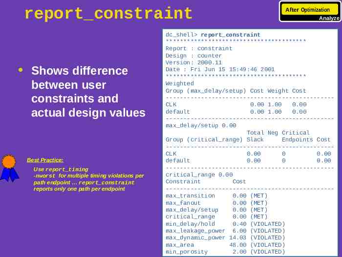
report constraint Shows difference between user constraints and actual design values Best Practice: Use report timing -nworst for multiple timing violations per path endpoint report constraint reports only one path per endpoint After Optimization Analyze dc shell report constraint **************************************** Report : constraint Design : counter Version: 2000.11 Date : Fri Jun 15 15:49:46 2001 **************************************** Weighted Group (max delay/setup) Cost Weight Cost -----------------------------------------------CLK 0.00 1.00 0.00 default 0.00 1.00 0.00 -----------------------------------------------max delay/setup 0.00 Total Neg Critical Group (critical range) Slack Endpoints Cost -----------------------------------------------CLK 0.00 0 0.00 default 0.00 0 0.00 -----------------------------------------------critical range 0.00 Constraint Cost -----------------------------------------------max transition 0.00 (MET) max fanout 0.00 (MET) max delay/setup 0.00 (MET) critical range 0.00 (MET) min delay/hold 0.40 (VIOLATED) max leakage power 6.00 (VIOLATED) max dynamic power 14.03 (VIOLATED) max area 48.00 (VIOLATED) min porosity 2.00 (VIOLATED)
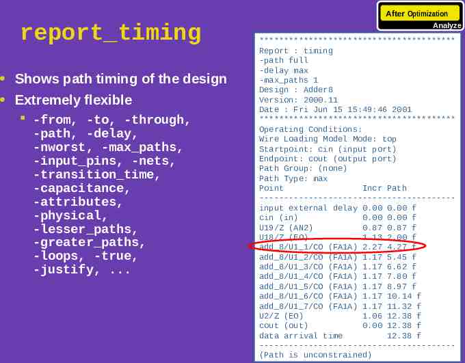
After Optimization report timing Shows path timing of the design Extremely flexible -from, -to, -through, -path, -delay, -nworst, -max paths, -input pins, -nets, -transition time, -capacitance, -attributes, -physical, -lesser paths, -greater paths, -loops, -true, -justify, . Analyze **************************************** Report : timing -path full -delay max -max paths 1 Design : Adder8 Version: 2000.11 Date : Fri Jun 15 15:49:46 2001 **************************************** Operating Conditions: Wire Loading Model Mode: top Startpoint: cin (input port) Endpoint: cout (output port) Path Group: (none) Path Type: max Point Incr Path ---------------------------------------input external delay 0.00 0.00 f cin (in) 0.00 0.00 f U19/Z (AN2) 0.87 0.87 f U18/Z (EO) 1.13 2.00 f add 8/U1 1/CO (FA1A) 2.27 4.27 f add 8/U1 2/CO (FA1A) 1.17 5.45 f add 8/U1 3/CO (FA1A) 1.17 6.62 f add 8/U1 4/CO (FA1A) 1.17 7.80 f add 8/U1 5/CO (FA1A) 1.17 8.97 f add 8/U1 6/CO (FA1A) 1.17 10.14 f add 8/U1 7/CO (FA1A) 1.17 11.32 f U2/Z (EO) 1.06 12.38 f cout (out) 0.00 12.38 f data arrival time 12.38 f ---------------------------------------(Path is unconstrained)
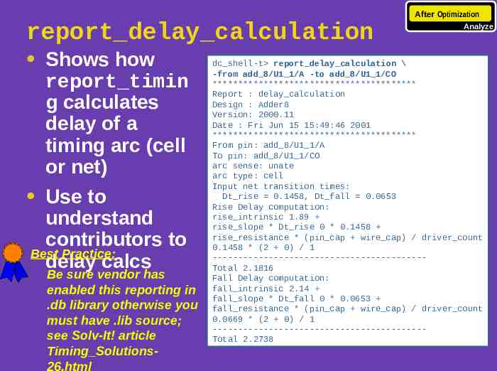
After Optimization report delay calculation Shows how report timin g calculates delay of a timing arc (cell or net) Use to understand contributors to Best Practice: delay calcs Be sure vendor has enabled this reporting in .db library otherwise you must have .lib source; see Solv-It! article Timing Solutions26.html Analyze dc shell-t report delay calculation \ -from add 8/U1 1/A -to add 8/U1 1/CO **************************************** Report : delay calculation Design : Adder8 Version: 2000.11 Date : Fri Jun 15 15:49:46 2001 **************************************** From pin: add 8/U1 1/A To pin: add 8/U1 1/CO arc sense: unate arc type: cell Input net transition times: Dt rise 0.1458, Dt fall 0.0653 Rise Delay computation: rise intrinsic 1.89 rise slope * Dt rise 0 * 0.1458 rise resistance * (pin cap wire cap) / driver count 0.1458 * (2 0) / 1 -----------------------------------------Total 2.1816 Fall Delay computation: fall intrinsic 2.14 fall slope * Dt fall 0 * 0.0653 fall resistance * (pin cap wire cap) / driver count 0.0669 * (2 0) / 1 -----------------------------------------Total 2.2738
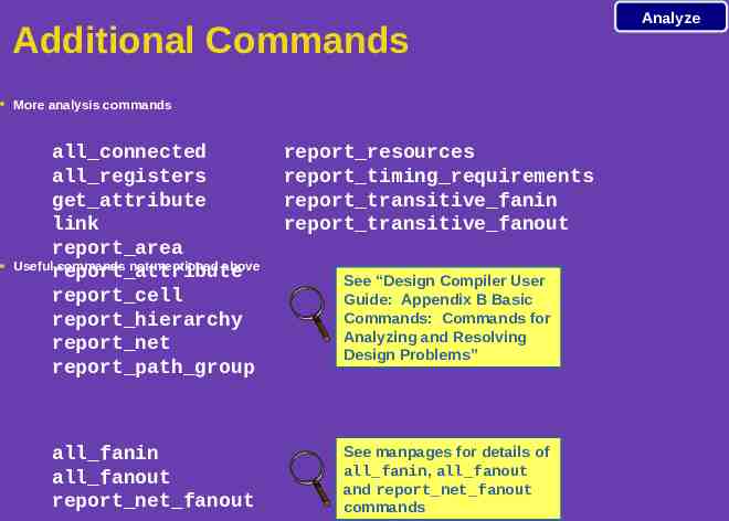
Additional Commands More analysis commands all connected all registers get attribute link report area commands not mentioned above Usefulreport attribute report cell report hierarchy report net report path group all fanin all fanout report net fanout report resources report timing requirements report transitive fanin report transitive fanout See “Design Compiler User Guide: Appendix B Basic Commands: Commands for Analyzing and Resolving Design Problems” See manpages for details of all fanin, all fanout and report net fanout commands Analyze
Analysis Summary Analyze Design Analysis Before optimization Verify user-defined constraints and attributes Check design consistency and timing path integrity During optimization Optionally customize compile log Optionally checkpoint compile run for debugging After optimization Verify timing and DRC constraints are satisfied Reference “DCUG Ch. 9” for specific debug scenarios Reference “DCUG Appendix B” for more commands Before Optimization During Optimization After Optimization Analyze
Take a Break!