Graphene-based Polymer Bulk Heterojunction Solar Cells Fei Yu and

21 Slides8.29 MB
Graphene-based Polymer Bulk Heterojunction Solar Cells Fei Yu and Vikram Kuppa School of Energy, Environmental, Biological and Medical Engineering College of Engineering and Applied Science University of Cincinnati APS March Meeting 2012, Boston
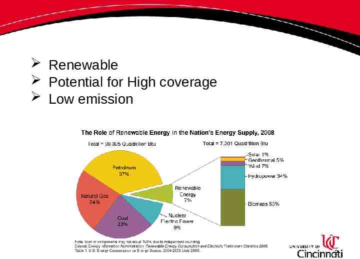
Solar Energy In Development Renewable Potential for High coverage Low emission 2
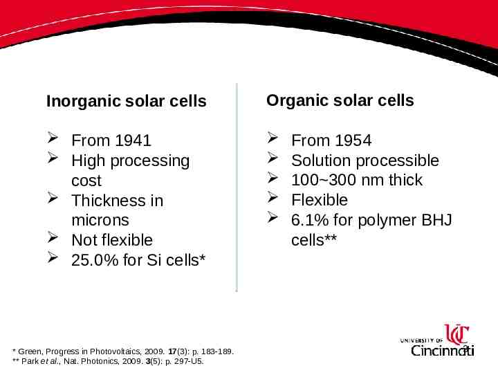
A comparison Inorganic solar cells Organic solar cells From 1941 High processing cost Thickness in microns Not flexible 25.0% for Si cells* * Green, Progress in Photovoltaics, 2009. 17(3): p. 183-189. ** Park et al., Nat. Photonics, 2009. 3(5): p. 297-U5. From 1954 Solution processible 100 300 nm thick Flexible 6.1% for polymer BHJ cells** 3
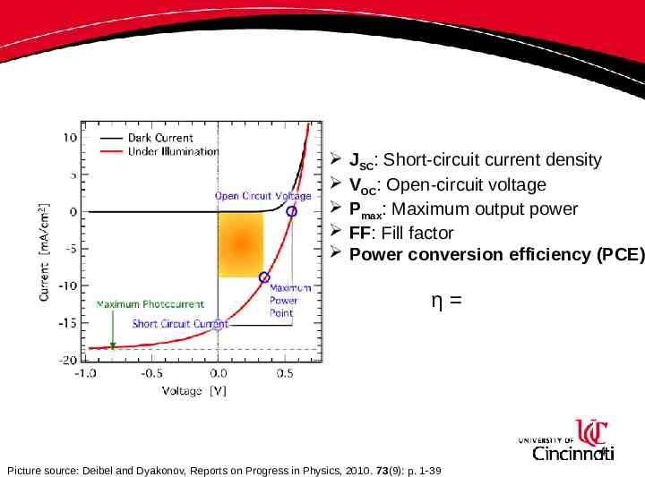
Solar Cell Parameters JSC: Short-circuit current density VOC: Open-circuit voltage Pmax: Maximum output power FF: Fill factor Power conversion efficiency (PCE) η 4 Picture source: Deibel and Dyakonov, Reports on Progress in Physics, 2010. 73(9): p. 1-39
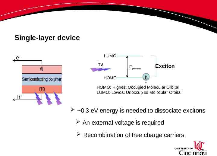
Polymer solar cells Single-layer device LUMO ehν Exciton Epolymer HOMO eh h HOMO: Highest Occupied Molecular Orbital LUMO: Lowest Unoccupied Molecular Orbital 0.3 eV energy is needed to dissociate excitons An external voltage is required Recombination of free charge carriers 5
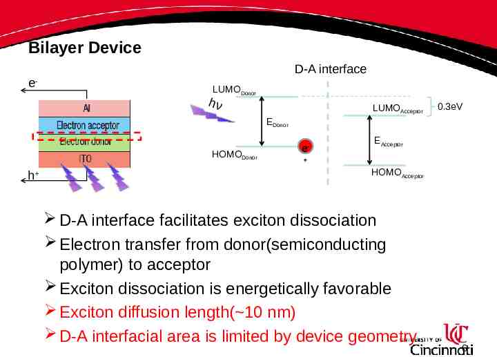
Bilayer Device e- D-A interface LUMODonor hν LUMOAcceptor 0.3eV EDonor HOMODonor h eh- EAcceptor HOMOAcceptor D-A interface facilitates exciton dissociation Electron transfer from donor(semiconducting polymer) to acceptor Exciton dissociation is energetically favorable Exciton diffusion length( 10 nm) D-A interfacial area is limited by device geometry 6
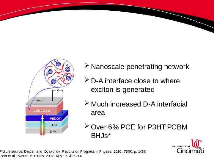
Bulk Heterojunction(BHJ) Solar Cells Nanoscale penetrating network D-A interface close to where exciton is generated Much increased D-A interfacial area Over 6% PCE for P3HT:PCBM BHJs* Picture source: Deibel and Dyakonov, Reports on Progress in Physics, 2010. 73(9): p. 1-39) Peet et al., Nature Materials, 2007. 6(7) : p. 497-500. 7
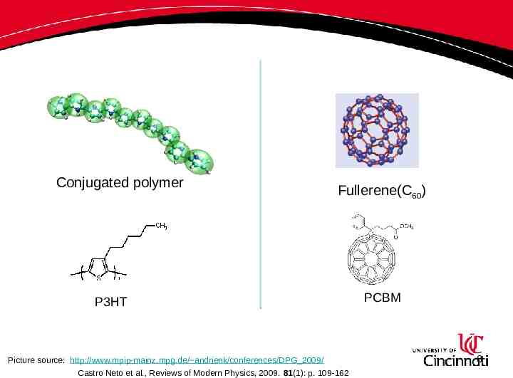
Donor Conjugated polymer Acceptor Fullerene(C60) P3HT Picture source: http://www.mpip-mainz.mpg.de/ andrienk/conferences/DPG 2009/ Castro Neto et al., Reviews of Modern Physics, 2009. 81(1): p. 109-162 PCBM 8
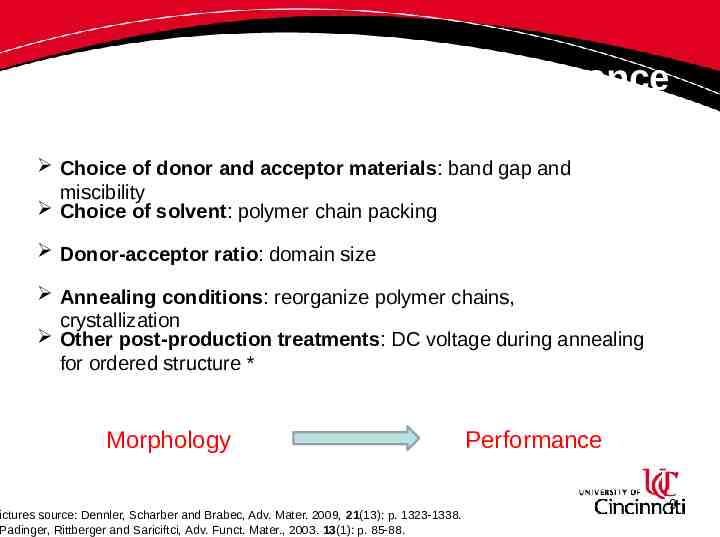
Factors Affecting BHJ Performance Choice of donor and acceptor materials: band gap and miscibility Choice of solvent: polymer chain packing Donor-acceptor ratio: domain size Annealing conditions: reorganize polymer chains, crystallization Other post-production treatments: DC voltage during annealing for ordered structure * Morphology ictures source: Dennler, Scharber and Brabec, Adv. Mater. 2009, 21(13): p. 1323-1338. Padinger, Rittberger and Sariciftci, Adv. Funct. Mater., 2003. 13(1): p. 85-88. Performance 9
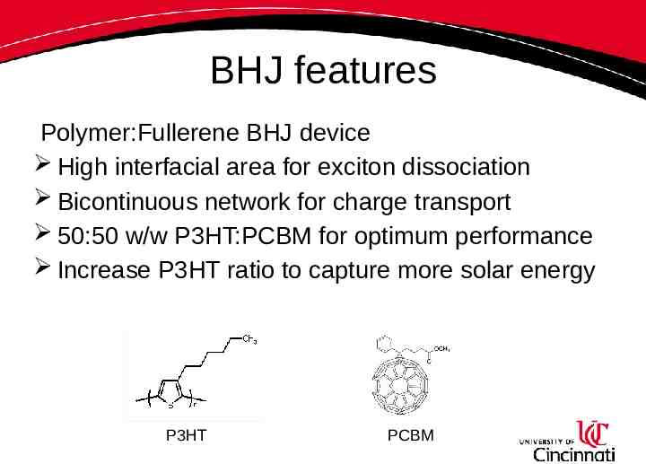
BHJ features Polymer:Fullerene BHJ device High interfacial area for exciton dissociation Bicontinuous network for charge transport 50:50 w/w P3HT:PCBM for optimum performance Increase P3HT ratio to capture more solar energy P3HT PCBM
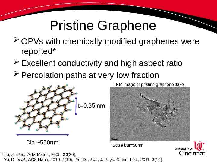
Pristine Graphene OPVs with chemically modified graphenes were reported* Excellent conductivity and high aspect ratio Percolation paths at very low fraction TEM image of pristine graphene flake t 0.35 nm Dia. 550nm Scale bar 50nm *Liu, Z. et al., Adv. Mater., 2008. 20(20), Yu, D. et al., ACS Nano, 2010. 4(10), Yu, D. et al., J. Phys. Chem. Lett., 2011. 2(10).
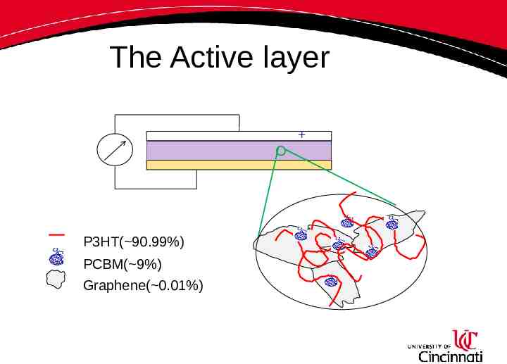
The Active layer P3HT( 90.99%) PCBM( 9%) Graphene( 0.01%)
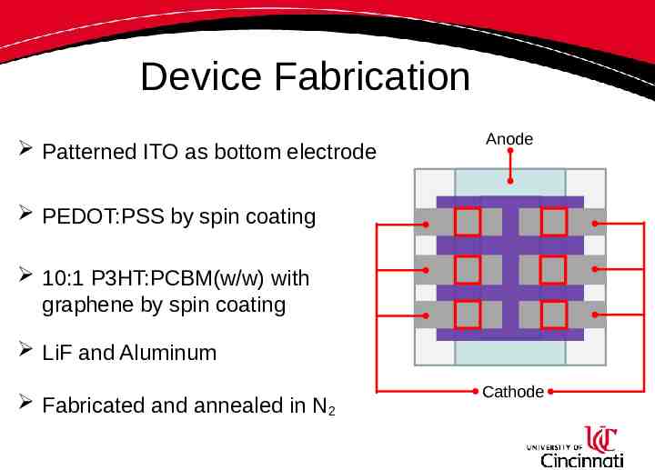
Device Fabrication Patterned ITO as bottom electrode Anode PEDOT:PSS by spin coating 10:1 P3HT:PCBM(w/w) with graphene by spin coating LiF and Aluminum Fabricated and annealed in N2 Cathode
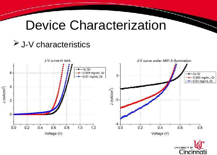
Device Characterization J-V characteristics
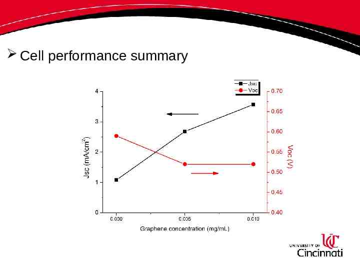
Cell performance summary
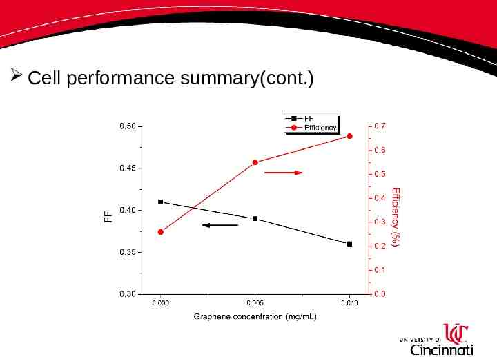
Cell performance summary(cont.)
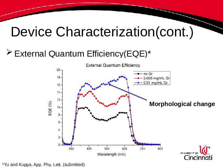
Device Characterization(cont.) External Quantum Efficiency(EQE)* Morphological change *Yu and Kuppa, App. Phy. Lett. (submitted)
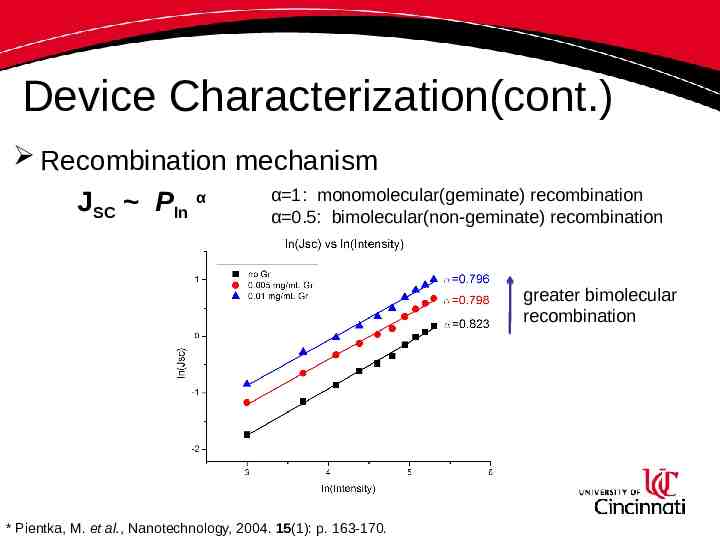
Device Characterization(cont.) Recombination mechanism JSC PIn α α 1: monomolecular(geminate) recombination α 0.5: bimolecular(non-geminate) recombination greater bimolecular recombination * Pientka, M. et al., Nanotechnology, 2004. 15(1): p. 163-170.
Conclusions Adding small fraction of graphene greatly enhances charge transport and leads to much better Jsc and Cells with more than 90% P3HT are viable Introduction of graphene in active layer leads to change of morphology Device physics change with increasing graphene fraction *Yu and Kuppa, App. Phy. Lett. (submitted)
Future Work Better dispersed and oriented graphene via morphological control Increase FF by reducing interfacial roughness Stability and device encapsulation FY and VKK thank UC and the URC for funding and support
Thank you!